Documentation of the UltraZohm#
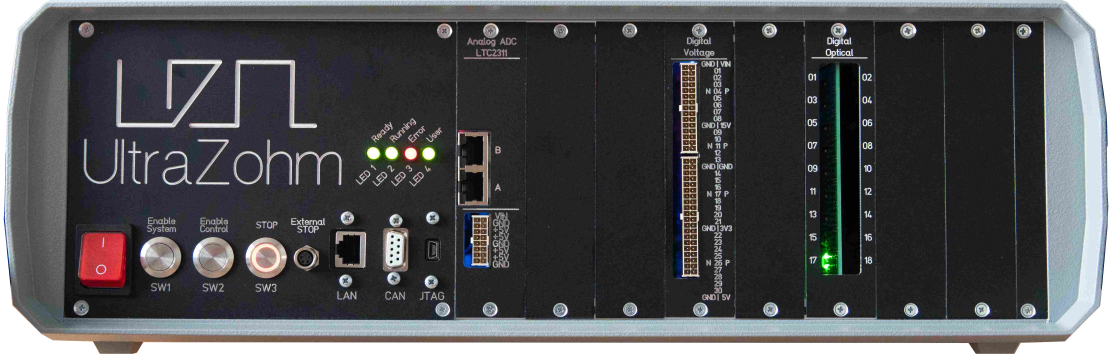
The UltraZohm is a powerful real-time computation platform for research, development, and rapid-control prototyping of power electronics and drive systems. Development is driven by researchers for researchers to establish a common control platform. Having a common platform enables the active research community to focus on publication and results, while platform development is a shared effort.
High Computational power
The UltraZohm is based on Xilinx Zynq UltraScale+ MPSoC (EG devices). These offer four ARM A53, two ARM R5, and a large FPGA (programmable logic - PL) in one System-on-a-Chip (SoC). The UltraScale is used with a System-on-a-Module (SoM) from Trenz Electronic GmbH. specifically the TE0808 with a ZU9EG device is the default and strongly recommended. Additionally, SoM with devices from 2EG (TE0803) to 15EG (TE0808) can be used with the UltraZohm framework out of the box using the Vivado build tcl scripts.
Hard real-time
The UltraZohm is designed to meet modern control systems’ timing requirements for power electronics. Thus, the control frequency of the real-time processor is in the range of \(10\,\mu s\) to \(100\,\mu s\), depending on the specific application. Additionally, many modern control algorithms such as model predictive control (MPC) and machine learning methods can be accelerated by using the PL (FPGA) of the UltraZohm. Therefore, the system is optimized for this approach.
Open Source
The UltraZohm is a platform with no black boxes and no barriers to your research. It is built with the intent to give users full control and the ability to easily adapt the system to their specific needs and preferences. Therefore, UltraZohm project is licensed by Apache 2.0 and the hardware is licensed under CERN-OHL-P. See License for details.
Modularity
The UltraZohm is modular regarding the UltraScale device to scale the computational power. The community continuously extends the platform with more hardware components, especially Adapter Cards for which templates and libraries exist. Furthermore, IP-Cores and software components are developed and shared, and included in the project.
Usability
The UltraZohm project thrives to be novice friendly with tutorials and an existing codebase. This is especially relevant to onboard new users with different backgrounds, ranging from bachelor, master’s, and PhD students to experienced engineers and developers. At the same time, the system is expert friendly with access to the last bit due to the lack of black boxes, access to the source code, and comprehensive documentation. In addition, there are multiple supported workflows for writing software (e.g., manually or using Embedded-Coder (C-Code)) and IP-Cores (manually, HDL-Coder (HDL), Vitis HLS).
Community
The UltraZohm community aims to connect researchers working on the same platform and solve infrastructure problems only once! We write and review code together, design PCBs, and share our knowledge regarding the UltraZohm, Xilinx UltraScale, electronics, control approaches, and many more! We welcome researchers from all around the world with an interest in the control of power electronics and electrical drives.
Documentation
Comprehensive and ever-growing documentation for the Ultrazohm on docs.ultrazohm.com.
Maintained & funded
Project development is funded by the BMBF with the research grant KI-Power and is actively maintained by the Institute ELSYS of TH Nuremberg as well as the Chair of High-Power Converter Systems (HLU) of TU Munich. In addition, researchers of TH Nuremberg and TU Munich founded the start-up Zohm Control GmbH to ensure the long term development of the system and to be able to distribute the fully assembled UltraZohm systems.
UltraZohm Community Slack#
The UltraZohm community is organized using Slack
Join the UltraZohm Slack
Acquiring an UltraZohm#
Please contact the commercial manufacturer Zohm Control GmbH of the UltraZohm to purchase a system
Alternatively, one can build and manufacture the system on their own since the project is licensed as open source and open source hardware (see License)
Note that while one is under no obligation to do so according to the licenses, it is advised to get in touch before building the system on your own
Write us at info@ultrazohm.com or ask in the Slack channel if you have questions regarding building or purchasing a system
Contributing#
We are accepting and welcoming contributions
Forking & creating a pull request is possible for everybody (see fork a repository documentation)
In principle, documentation, software, and even IP-Cores can be developed and contributed without physical access to an UltraZohm
For IP-Cores, developing with a generic UltraScale development kit is advised
While we try to reduce the barrier for contributions, physical access to an UltraZohm is often required
Contributes can get in contact by mail or Slack to the maintainers to get write access to the repository and switch to a feature-branch workflow (see Contribution Workflow)
Open in Gitpod for contributing without tool setup
Research#
The primary use of the UltraZohm is the research of modern control algorithms for power electronics and drive systems:
Model predictive control of electric drives
Model predictive control of power electronics systems
Renewable energy systems
Multilevel converter including Modular Multilevel Converter (MMC)
Multi-phase motors (m>3)
Special electric motor designs (e.g., transverse flux machine, synchronous reluctance motor)
Machine Learning in drive systems
Literature about the UltraZohm#
Literature using the UltraZohm#
Real-Time Implementation of Long-Horizon Direct Model Predictive Control on an Embedded System
Real-Time Inference of Neural Networks on FPGAs for Motor Control Applications
Modeling of an Interleaved DC-DC Boost Converter for a Direct Model Predictive Control Strategy
Implementation of a Long-Horizon Model Predictive Control Algorithm on an Embedded System
Design Guidelines of Rapid Control Prototyping Systems for Power Electronics and Electrical Drives
Design, Construction and Measurement of a Laminated Transverse Flux Machine
License#
The project is licensed under the Apache 2.0 license. See LICENSE for details. The source of the documentation is located in ultrazohm_sw/docs.
The hardware is documented in Carrier Board and Adapter Cards including schematics and assembly files. Additionally, the source files of the PCBs is available in the PCB-Design project. Note that due to the specifics of Bitbucket, this project is only visible to users that are part of the UltraZohm workspace. The individual repositories of the PCB projects can be accessed directly if one is not part of the Ultrazohm workspace, e.g. DAC-Card repository. The documentation pages of the PCB links to their respective repository. The preferred license for hardware within the UltraZohm project is the CERN Open Hardware License Version 2 - Permissive (CERN-OHL-P). The UltraZohm project uses Altium for PCB design.
Note
If you use the UltraZohm project or parts of it for your own systems, research, and publications, referencing the UltraZohm project is greatly appreciated!
Syllabus#
Contents: