Inverter Adapter#
This IP core provides a well defined and highly sophisticated interface for inverter adapter boards for the UltraZohm (e.g. MOSFET 48V Inverter (Digital adapter slot)). It provides many useful features:
6 gate signal outputs
1 gate enable signal output. The output gate enable is only high, when both the
software enableand theUZ-PWM-Enableare high.6 over current (OC) input signals
6 fault (FAULT) input signals
6 pwm input signals for measuring e.g. chip temperatures. Duty cycle is calculated to degrees celsius in software driver. To save execution time, only one temperature signal is read out per cycle.
4 diagnostic input signals (e.g. power good or signal valid of current amplifiers)
Hardware Interface Definition#
Usage of the IP core requires a defined pin mapping on the respective inverter adapter board, as shown in the table below.
Adapter Card Pin |
Net Name |
Signal Description |
Signal Type |
Direction seen from Adapter Board |
|---|---|---|---|---|
DIG_IO_00 |
PWM H1# |
Gate H1 |
PWM/Direct |
Input |
DIG_IO_01 |
PWM L1# |
Gate L1 |
PWM/Direct |
Input |
DIG_IO_02 |
PWM H2# |
Gate H2 |
PWM/Direct |
Input |
DIG_IO_03 |
PWM L2# |
Gate L2 |
PWM/Direct |
Input |
DIG_IO_04 |
PWM H3# |
Gate H3 |
PWM/Direct |
Input |
DIG_IO_05 |
PWM L3# |
Gate L3 |
PWM/Direct |
Input |
DIG_IO_06 |
I1 DIAG |
Diagnostic Signal of current i1 |
Level, low active |
Output |
DIG_IO_07 |
H1 Temp |
Temperature feedback H1 |
PWM |
Output |
DIG_IO_08 |
I2 DIAG |
Diagnostic Signal of current i2 |
Level, low active |
Output |
DIG_IO_09 |
L1 Temp |
Temperature feedback L1 |
PWM |
Output |
DIG_IO_10 |
I3 DIAG |
Diagnostic Signal of current i3 |
Level, low active |
Output |
DIG_IO_11 |
L1 OC |
Over current indicator L1 |
Level, low active |
Output |
DIG_IO_12 |
I DIAG |
Diagnostic Signal of current i_dc |
Level, low active |
Output |
DIG_IO_13 |
L1 FAULT |
Fault indicator L1 |
Level, low active |
Output |
DIG_IO_14 |
PWM EN |
Enable Gate signals |
Level, high active |
Input |
DIG_IO_15 |
H1 OC |
Over current indicator H1 |
Level, low active |
Output |
DIG_IO_16 |
||||
DIG_IO_17 |
H1 FAULT |
Fault indicator H1 |
Level, low active |
Output |
DIG_IO_18 |
H3 Temp |
Temperature feedback H3 |
PWM |
Output |
DIG_IO_19 |
H2 Temp |
Temperature feedback H2 |
PWM |
Output |
DIG_IO_20 |
L3 Temp |
Temperature feedback L3 |
PWM |
Output |
DIG_IO_21 |
L2 Temp |
Temperature feedback L2 |
PWM |
Output |
DIG_IO_22 |
L3 OC |
Over current indicator L3 |
Level, low active |
Output |
DIG_IO_23 |
L2 OC |
Over current indicator L2 |
Level, low active |
Output |
DIG_IO_24 |
L3 FAULT |
Fault indicator L3 |
Level, low active |
Output |
DIG_IO_25 |
L2 FAULT |
Fault indicator L2 |
Level, low active |
Output |
DIG_IO_26 |
H3 OC |
Over current indicator H3 |
Level, low active |
Output |
DIG_IO_27 |
H2 OC |
Over current indicator H2 |
Level, low active |
Output |
DIG_IO_28 |
H3 FAULT |
Fault indicator H3 |
Level, low active |
Output |
DIG_IO_29 |
H2 FAULT |
Fault indicator H2 |
Level, low active |
Output |
Organization of the sources#
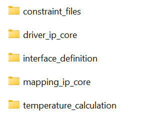
Fig. 431 Folder structure of the sources in ip_cores/uz_d_inverter_adapter/#
Folder structure of the sources in ip_cores/uz_d_inverter_adapter/:
constraint_filescontains ready to use Vivado constraint files for usage of the adapter board interface in any digital slot D1..D4driver_ip_corecontains the IP core with which the user communicates via the software driverinterface_definitioncontains the Vivado interface definition using the pin names from the constraint filesmapping_ip_corecontains the IP core that maps and organizes signals from the adapter boardtemperature_calculationcontains excel sheets for determination of the linear interpolation equation to get temperatures in degrees celsius from a duty cycle value of a PWM signal. The parameters of the equation depend on the circuit design and/or the used power electronic switch and have to be determined by the adapter board developer carefully
Example Usage#
The following step-by-step description shall guide the user in order to properly implement the IP core and the respective interface and software drivers
Vivado Block Design#
First, IP cores have to be added to the block design in vivado:
Create a hierarchy (e.g. inside the already existing
uz_userhierarchy) in the block designright click -> Create Hierarchy...in order to keep the block design clean and name ituz_inverter_adapterInside this new hierarchy click on the plus (
+) button to add new ip and first add theuz_d_inverter_adapterIP coreNext,
right click -> Add IP...and add theuz_inverter_adapter_mapping_v1_0IP coreConnect all signals between those two IP cores that have equal names
Add an additional AXI Port on the next reachable
AXI SmartConnectIP core and connect it to theuz_d_inverter_adapterIP core, as well as clocks and resets. The IP core is designed for a 100 MHz clock rate. Do not forget to assign a base address in the Address Editor.Provide gate signals to the
uz_inverter_adapter_mapping_v1_0(e.g. by slicing them from the D1_OUT port of theuz_digital_adapterhierarchy)
After those steps the block design looks like this:
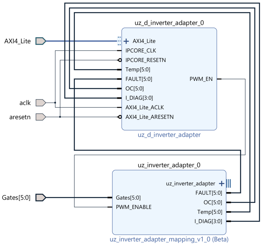
Fig. 432 Block design after steps above#
PWM Enable#
Second, the PWM-Enable of the UZ has to be connected to the IP core.
In the top hierarchy (
Diagram) expand theuz_useranduz_inverter_adapterhierarchy with the (+) in the top left corner.Connect the
PWM_UZ_EnablePort with theD1_OUT_29Port of the uz_system hierarchy. This is the PWM-Enable port of the UZ.

Fig. 433 Block design after steps above#
Vivado Interface#
Third, the interface between the IP cores and the physical pins has to be implemented:
Inside the top level block design
right click -> Create Interface Pin...Name the interface according to the digital slot where you plan to use the inverter adapter board (e.g.
D1)In the search field type in
inverter. There should be a result calleduz_inverter_adapter_rtl:1.0in theVLNVcolumn. Select it and pressOKConnect the interface pin
D1withuz_inverter_adapterinterface port at theuz_inverter_adapter_mapping_v1_0IP core (unfolding the hierarchies with the+buttons in their upper left corner makes it really easy)
After those steps the block design inside your hierarchy looks like this:
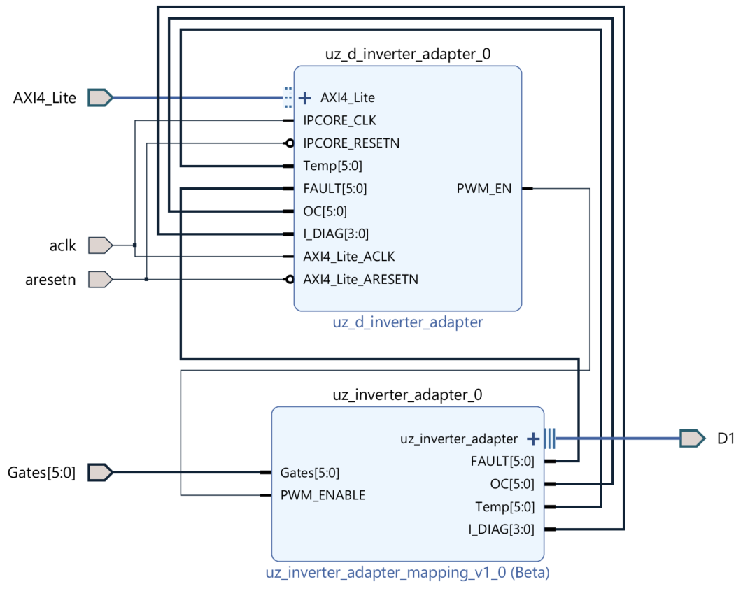
Fig. 434 Block design after steps above#
The top level block design looks like this
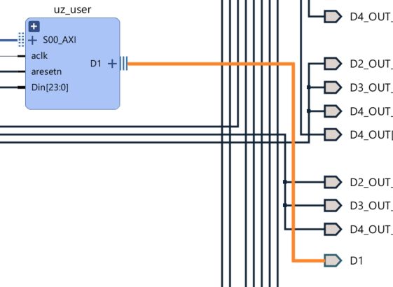
Fig. 435 Top level block design after steps above#
Due to our interface using all 30 pins of one digital slot, make sure no other pins (e.g. D1_OUT_26 to D1_OUT_29 in our case) are present in the block design. If yes, simply delete them.
Constraints#
Third, the interface definition we connected in the step before uses specific names for the signals and pins. Those have to match the names of the respective constraint file of the respective digital slot.
In the subfolder constraint_files inside the IP core sources (see Fig. 431) ready to use constraint files are prepared for this purpose:
Open the respective constraint file (in our example the one for D1:
Digital_D1_packed.xdc)Copy everything inside the file
Paste and overwrite everything inside the constraint file in your vivado project
Save the changed file in your vivado project
After those steps the file looks like this:
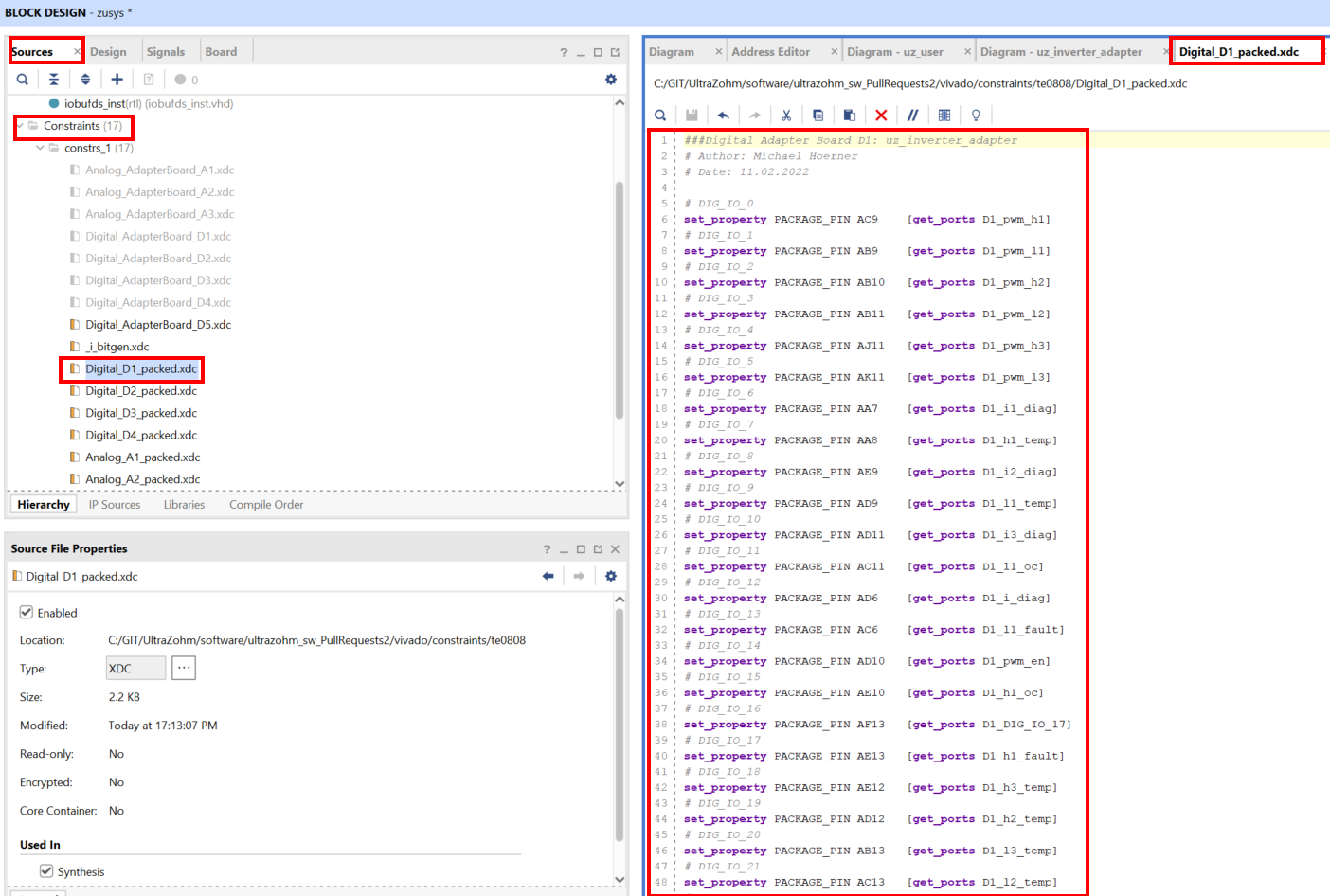
Fig. 436 Constraint file after copy paste#
CPLD program#
Keep in mind, that a proper CPLD program for this interface and respective adapter boards is required. It can be found in the cpld_lattice repository
under uz_d_3ph_inverter
Software driver#
For interacting with the IP core, the following step-by-step example shows a way of implementing one instance of the software driver.
In Vitis, in the Baremetal project under the folder
hw_initcreate a new fileuz_inverter_adapter_init.cInclude necessary files and create
configandoutputstructs as well as an init function for one or more instances:
#include "../include/uz_inverter_adapter_init.h"
#include "../uz/uz_HAL.h"
#include "../uz/uz_global_configuration.h"
#include "xparameters.h"

static struct uz_inverter_adapter_config_t uz_inverter_adapter_config_d1 = {
               .base_address = XPAR_UZ_USER_UZ_INVERTER_ADAPTER_UZ_D_INVERTER_ADAPTER_0_BASEADDR,
               .ip_clk_frequency_Hz = 100000000,
               .linear_interpolation_params = {162.35f, 20.107f}
};

static struct uz_inverter_adapter_outputs_t uz_inverter_adapter_outputs_d1 = {
   .PWMdutyCycNormalized_H1 = 0.0f,
   .PWMdutyCycNormalized_L1 = 0.0f,
   .PWMdutyCycNormalized_H2 = 0.0f,
   .PWMdutyCycNormalized_L2 = 0.0f,
   .PWMdutyCycNormalized_H3 = 0.0f,
   .PWMdutyCycNormalized_L3 = 0.0f,
   .ChipTempDegreesCelsius_H1 = 0.0f, /**< Chip temperature of H1 in degrees celsius */
   .ChipTempDegreesCelsius_L1 = 0.0f, /**< Chip temperature of L1 in degrees celsius */
   .ChipTempDegreesCelsius_H2 = 0.0f, /**< Chip temperature of H2 in degrees celsius */
   .ChipTempDegreesCelsius_L2 = 0.0f, /**< Chip temperature of L2 in degrees celsius */
   .ChipTempDegreesCelsius_H3 = 0.0f, /**< Chip temperature of H3 in degrees celsius */
   .ChipTempDegreesCelsius_L3 = 0.0f, /**< Chip temperature of L3 in degrees celsius */
   .OC = 0U,
   .OC_H1 = 0U, /**< Over current OC fault signal of H1 */
   .OC_L1 = 0U, /**< Over current OC fault signal of L1 */
   .OC_H2 = 0U, /**< Over current OC fault signal of H2 */
   .OC_L2 = 0U, /**< Over current OC fault signal of L2 */
   .OC_H3 = 0U, /**< Over current OC fault signal of H3 */
   .OC_L3 = 0U, /**< Over current OC fault signal of L3 */
   .FAULT = 0U,
   .FAULT_H1 = 0U, /**< FAULT signal of H1 */
   .FAULT_L1 = 0U, /**< FAULT signal of L1 */
   .FAULT_H2 = 0U, /**< FAULT signal of H2 */
   .FAULT_L2 = 0U, /**< FAULT signal of L2 */
   .FAULT_H3 = 0U, /**< FAULT signal of H3 */
   .FAULT_L3 = 0U, /**< FAULT signal of L3 */
   .I_DIAG = 0U,
   .I_DC_DIAG = 0U, /**< Diagnostic signal of current amplifier for DC current */
   .I1_DIAG = 0U, /**< Diagnostic signal of current amplifier for phase a current */
   .I2_DIAG = 0U, /**< Diagnostic signal of current amplifier for phase b current */
   .I3_DIAG = 0U /**< Diagnostic signal of current amplifier for phase c current */
};

uz_inverter_adapter_t* initialize_uz_inverter_adapter_on_D1(void) {
       return(uz_inverter_adapter_init(uz_inverter_adapter_config_d1, uz_inverter_adapter_outputs_d1));
}
3. When using the pwm measurement feature of the IP core (e.g. for measuring temperatures), set the values in the above linear_interpolation_params struct according to the linear interpolation function that calculates readable
SI-values from the duty cycle information. The example values above of 162.35 and 20.107 are valid for the uz_d_gan_inverter adapter board and the respective TI LMG3425 GaN switch. See also the folder temperature_calculation in the sources of this IP core driver for details.
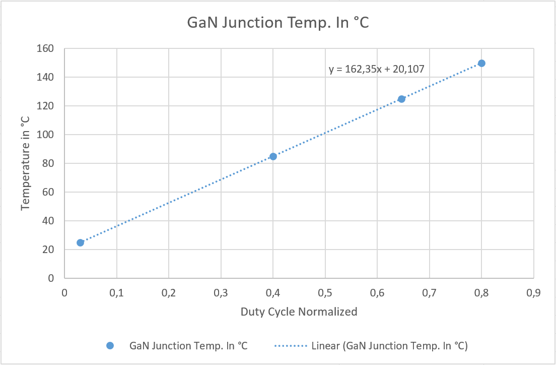
Fig. 437 Determination of values for linear_interpolation_params struct#
In Vitis, in the Baremetal project under the folder
includecreate a new fileuz_inverter_adapter_init.h.Include necessary files and declare the init functions for one or more instances:
#pragma once
#include "../IP_Cores/uz_inverter_adapter/uz_inverter_adapter.h"

uz_inverter_adapter_t* initialize_uz_inverter_adapter_on_D1(void);
In Vitis, in the Baremetal project in
main.hinclude necessary header files:
#include "IP_Cores/uz_inverter_adapter/uz_inverter_adapter.h"
#include "include/uz_inverter_adapter_init.h"
In Vitis, in the Baremetal project in
globalData.hinclude necessary header file:
#include "IP_Cores/uz_inverter_adapter/uz_inverter_adapter.h"
In the same file, add an object pointer variable in the
object_pointers_tstruct:
 typedef struct {
 ...
 uz_inverter_adapter_t* inverter_d1;
 }object_pointers_t;
In Vitis, in the Baremetal project in
main.cinitialize an instance:
   case init_ip_cores:
   ...
   Global_Data.objects.inverter_d1 = initialize_uz_inverter_adapter_on_D1();
   break;
10. For reading signals and states of the IP core use the function uz_inverter_adapter_get_outputs which updates the states and returns them in the form of a uz_inverter_adapter_outputs_t struct. This
way you can get the states of the status signals of the driver e.g. for assigning them into the Global_Data struct.
 void ISR_Control(void *data)
 {
   uz_SystemTime_ISR_Tic(); // Reads out the global timer, has to be the first function in the isr
   ReadAllADC();
   update_speed_and_position_of_encoder_on_D5(&Global_Data);

   Global_Data.av.inverter_outputs_d1 = uz_inverter_adapter_get_outputs(Global_Data.objects.inverter_d1);
 ..
  }
In order to enable the gates of the power electronics use the function uz_inverter_adapter_set_PWM_EN. After power up, the gates are disabled by default.
uz_inverter_adapter_set_PWM_EN(Global_Data.objects.inverter_d1, true);
Reference#
-
typedef struct uz_inverter_adapter_t uz_inverter_adapter_t#
Data type for object uz_inverter_adapter.
-
struct linear_interpolation_params_t#
Struct for linear interpolation parameters using a function of the form y=ax+b.
- Param a:
Gradient
- Param b:
Offset
-
struct uz_inverter_adapter_config_t#
Configuration struct for uz_inverter_adapter.
Public Members
-
uint32_t base_address#
Base address of the IP-Core instance to which the driver is coupled
-
uint32_t ip_clk_frequency_Hz#
Clock frequency of the IP-Core
-
linear_interpolation_params_t linear_interpolation_params#
Parameters for linear interpolation of temperature measurement
-
uint32_t base_address#
-
struct uz_inverter_adapter_outputs_t#
Struct to return and read the outputs of uz_inverter_adapter.
Public Members
-
float ChipTempDegreesCelsius_H1#
Chip temperature of H1 in degrees celsius
-
float ChipTempDegreesCelsius_L1#
Chip temperature of L1 in degrees celsius
-
float ChipTempDegreesCelsius_H2#
Chip temperature of H2 in degrees celsius
-
float ChipTempDegreesCelsius_L2#
Chip temperature of L2 in degrees celsius
-
float ChipTempDegreesCelsius_H3#
Chip temperature of H3 in degrees celsius
-
float ChipTempDegreesCelsius_L3#
Chip temperature of L3 in degrees celsius
-
bool OC_H1#
Over current OC fault signal of H1
-
bool OC_L1#
Over current OC fault signal of L1
-
bool OC_H2#
Over current OC fault signal of H2
-
bool OC_L2#
Over current OC fault signal of L2
-
bool OC_H3#
Over current OC fault signal of H3
-
bool OC_L3#
Over current OC fault signal of L3
-
bool FAULT_H1#
FAULT signal of H1
-
bool FAULT_L1#
FAULT signal of L1
-
bool FAULT_H2#
FAULT signal of H2
-
bool FAULT_L2#
FAULT signal of L2
-
bool FAULT_H3#
FAULT signal of H3
-
bool FAULT_L3#
FAULT signal of L3
-
bool I_DC_DIAG#
Diagnostic signal of current amplifier for DC current
-
bool I1_DIAG#
Diagnostic signal of current amplifier for phase a current
-
bool I2_DIAG#
Diagnostic signal of current amplifier for phase b current
-
bool I3_DIAG#
Diagnostic signal of current amplifier for phase c current
-
float ChipTempDegreesCelsius_H1#
-
void uz_inverter_adapter_update_states(uz_inverter_adapter_t *self)#
updates the states and signals read from the ip-core, called by uz_inverter_adapter_get_outputs function
- Parameters:
self – Pointer to the instance
User interfaces#
-
uz_inverter_adapter_t *uz_inverter_adapter_init(struct uz_inverter_adapter_config_t config, struct uz_inverter_adapter_outputs_t outputs)#
Initializes an instance of the uz_inverter_adapter driver.
- Parameters:
config – Configuration values for the IP-Core
outputs – Output values of the IP-Core
- Returns:
Pointer to initialized instance
-
void uz_inverter_adapter_set_PWM_EN(uz_inverter_adapter_t *self, bool pwm_en_onoff)#
sets the enable pin for the gate drivers
- Parameters:
self – Pointer to the instance
pwm_en_onoff – enables (true) or disables (false) the gates
-
struct uz_inverter_adapter_outputs_t uz_inverter_adapter_get_outputs(uz_inverter_adapter_t *self)#
returns the state and signals of the output struct
- Parameters:
self – Pointer to the instance
Helper functions#
-
bool extract_state_from_bitpattern(uint32_t bitpattern, uint32_t position)#
returns one status bit from concatenated bit patterns, called by uz_inverter_adapter_get_outputs function
- Parameters:
bitpattern – concatenated bit pattern from which a status bit should be returned
position – defines the position of the status bit that should be returned bitpattern: (MSB)31 … 0(LSB)
-
float uz_inverter_adapter_PWMdutyCycNormalized_to_DegreesCelsius(uz_inverter_adapter_t *self, float dutyCycleNormalized)#
Calculates chip temperature from duty cycle,
called by uz_inverter_adapter_get_outputs function.
- Parameters:
self – Pointer to driver instance
dutyCycleNormalized – measured duty cycle of the PWM temperature signal
- Returns:
float value of chip temperature in degrees Celsius