ADC MAX11331 V1#
Introduction#
The IP core ADC_MAX11331 in version 1 is designed to read the ADCs which are located on the analog adapter board and to further process the values obtained from the ADCs.
The IP core features an AXI4 Lite interface for settings and software control.
The conversion can be triggered by using the hardware port
enable_measurefor real-time control.The IP core ADC_MAX11331 (in contrast to the IP core LTC2311) does not process (offset and conversion factor) the raw values further to an SI value, instead it only provides the RAW value
raw_measured_data.The raw value from the ADC is a
std_logic_vectorat the hardware interface of the IP core.
Features#
Up to 6 independent Serial Peripheral Interface (SPI) Masters can communicate with up to 6 independent MAX11331 ADC chips, each capable of sampling up to 16 synchronous channels. In total up to 96 individual ADC channels are theoretically possible with one IP-Core instance.
Each SPI Master (ADC chip) is able to read 16 single-ended or 8 differential channels. In order to interact with the analog adapter board, the interface must be set to differential.
The IP-Core does the following tasks:
Initialize the 1-6 MAX11331 ADC chip(s)
Validate SPI communication to the ADC chip(s)
Send data to the ADC chip(s) in order to sample 8 differential channels (or alternatively 16 single-ended channels)
Read back the 16(8) ADC channels, which are sampled one after another.
Sampling#
Each ADC chip contains one initial message and afterwards:
In single-ended case: Each ADC contains 16 channels, which are sampled one after each other. Hence, 16 +1 SPI messages are required to sample and send the 16 channel values.
In differential case: Each ADC contains 8 channels, which are sampled one after each other. Hence, 8 +1 SPI messages are required to sample and send the 8 channel values.
The initial (extra) message is required since the first message tells the ADC which channel should be sampled. Afterwards, thus from the second message ongoing the data are send (first only the odd channel numbers and than the even channel numbers)
Configuration#
The IP-Core instance needs the processor to set the registers of the MAX11331 ADC chip for the following reasons:
Configure the SPI-Clock divider
Configure how many MAX11331 chips are connected (number of Masters). On analog adapter board are three MAX11331 ADC chips, thus three Masters, used.
The settings required by the registers in the ADC chip(s) are set in individual SPI messages with the name of the respective register, so it is easy to change the initialization using the data sheet if necessary.
Offset and conversion factor are configurable by software individually for each ADC in
main.cOffset is set to zero by default
Conversion factor is set to 10/6.65*3.3 = 4.96241 by default due to the gain of amplifier circuit described in the hardware section of uz_a_max11331 adapter card .
SPI Interface#
A bidirectional communication from the ADC to FPGA is possible, i.e., read and write SPI.
CPHA,CPOL,clk_divandadc_delay_offsetof the SPI interface are configurable by softwareThe
SCLKfrequency scales with \(f_{SCLK} = \frac{ f_{SystemClock} }{2 \cdot (CLK\_DIV + 1)}\)
IP-Core clk frequency is typically 100MHz:
The SPI-Clock is generated internally by logic of clock divider. You can change its value from the IP-core using the SPI-Clock divider.
Clock divider 0x1, set SPI-Clock to 50Mhz.
Clock divider 0x2, set SPI-Clock to 25Mhz.
Clock divider 0x3, set SPI-Clock to 16.6Mhz and so on.
The SPI SCK frequency will be given by: IP-Core clk frequency / (2^(clock divider))
The SPI SCK frequency of 16.67MHZ(= 0x3) is used in default.
ADC Trigger#
Continuous and hardware (PL) triggered operation mode can be chosen by
trigger_mode. Hardware (PL) triggered interface is designed for real-time requirements in time-critical applications:There is an input pin to trigger the start sampling when it has the value
1.Changing the trigger value during sampling has no effect.
The trigger pin is only read when there is no sampling active.
If the trigger pin is fix to
1, the IP-Core will continuously sample the 16(8) channels using the 17(9) messages explained before.It is important to note that the 16(8) channels of an ADC chip are sampled in sequence, which must be known if the data is to be used in the control loop.
The IP core updates all channel outputs as soon as the last channel has been sampled and read. Therefore you will not notice how the channels are actually sampled, but all 16(8) channels are updated simultaneously at the IP core output in the FPGA.
Output is supplied to the PL-ports of the IP-Core as well as to the AXI4 over the TCM.
AXI Interface#
Table Interface of adc_max11331 IP-Core lists all input and output ports (AXI and external port) that are present in the IP-Core.
Port Name |
Port Type |
Data Type |
Target Platform Interfaces |
Range |
Unit |
Function |
|---|---|---|---|---|---|---|
miso[5:0] |
Input |
bool |
External Signal |
SPI communication Master-Input-Slave-Output signal: Here the data of 1-6 MAX11331 chips are received. Default only 1 chip is present. |
||
sclk |
Output |
bool |
External Signal |
SPI communication clock signal for the MAX11331 chip. |
||
mosi |
Output |
bool |
External Signal |
SPI communication Master- Output-Slave-Input signal. This signal is used to configure the MAX11331 chip. If several MAX11331 chips are present on the SPI line all of them receive the same configuration. |
||
ss_n |
Output |
bool |
External Signal |
SPI communication slave-select signal. If several MAX11331 chips are present on the SPI line all of them receive the same chip-select. |
||
enable_measure |
Input |
bool |
External Signal |
Trigger to start ADC sampling of its 16 (8) channels. The initialization by the R5 processor must have been completed before (init_done pin is high) to be able to read out the results in the ADC chip by the IP-core. |
||
init_done |
Output |
bool |
External Signal |
Flag to indicate the end of initialization. |
||
meas_done |
Output |
bool |
External Signal |
Flag to indicate the end of 16 (8) channels sampling. |
||
new_data |
Output |
bool |
External Signal |
Flag to indicate the update of all channel data vector. |
||
error |
Output |
bool |
External Signal |
Flag to indicate an error in initialization echo read. |
||
clk_division |
Input |
fix4_En0 |
AXI4-Lite |
0x1… |
divider |
Setting the clock divider using the spi_cfgr function. |
adc_selector_forceinit |
Input |
fix6_En0 |
AXI4-Lite |
0x1… |
divider |
Selecting the master used by using the check_echo_of_master function. |
ch0[15:0] |
Output |
sfix16_En0 |
External Signal |
4096 |
Raw |
ADC value of channel 0 |
ch1[15:0] |
Output |
sfix16_En0 |
External Signal |
4096 |
Raw |
ADC value of channel 1 |
ch2[15:0] |
Output |
sfix16_En0 |
External Signal |
4096 |
Raw |
ADC value of channel 2 |
ch3[15:0] |
Output |
sfix16_En0 |
External Signal |
4096 |
Raw |
ADC value of channel 3 |
ch4[15:0] |
Output |
sfix16_En0 |
External Signal |
4096 |
Raw |
ADC value of channel 4 |
ch5[15:0] |
Output |
sfix16_En0 |
External Signal |
4096 |
Raw |
ADC value of channel 5 |
ch6[15:0] |
Output |
sfix16_En0 |
External Signal |
4096 |
Raw |
ADC value of channel 6 |
ch7[15:0] |
Output |
sfix16_En0 |
External Signal |
4096 |
Raw |
ADC value of channel 7 |
ch8[15:0] |
Output |
sfix16_En0 |
External Signal |
4096 |
Raw |
ADC value of channel 8 |
ch9[15:0] |
Output |
sfix16_En0 |
External Signal |
4096 |
Raw |
ADC value of channel 9 |
ch10[15:0] |
Output |
sfix16_En0 |
External Signal |
4096 |
Raw |
ADC value of channel 10 |
ch11[15:0] |
Output |
sfix16_En0 |
External Signal |
4096 |
Raw |
ADC value of channel 11 |
ch12[15:0] |
Output |
sfix16_En0 |
External Signal |
4096 |
Raw |
ADC value of channel 12 |
ch13[15:0] |
Output |
sfix16_En0 |
External Signal |
4096 |
Raw |
ADC value of channel 13 |
ch14[15:0] |
Output |
sfix16_En0 |
External Signal |
4096 |
Raw |
ADC value of channel 14 |
ch15[15:0] |
Output |
sfix16_En0 |
External Signal |
4096 |
Raw |
ADC value of channel 15 |
Default Setups#
The MAX11331 can be configured in multiple ways as
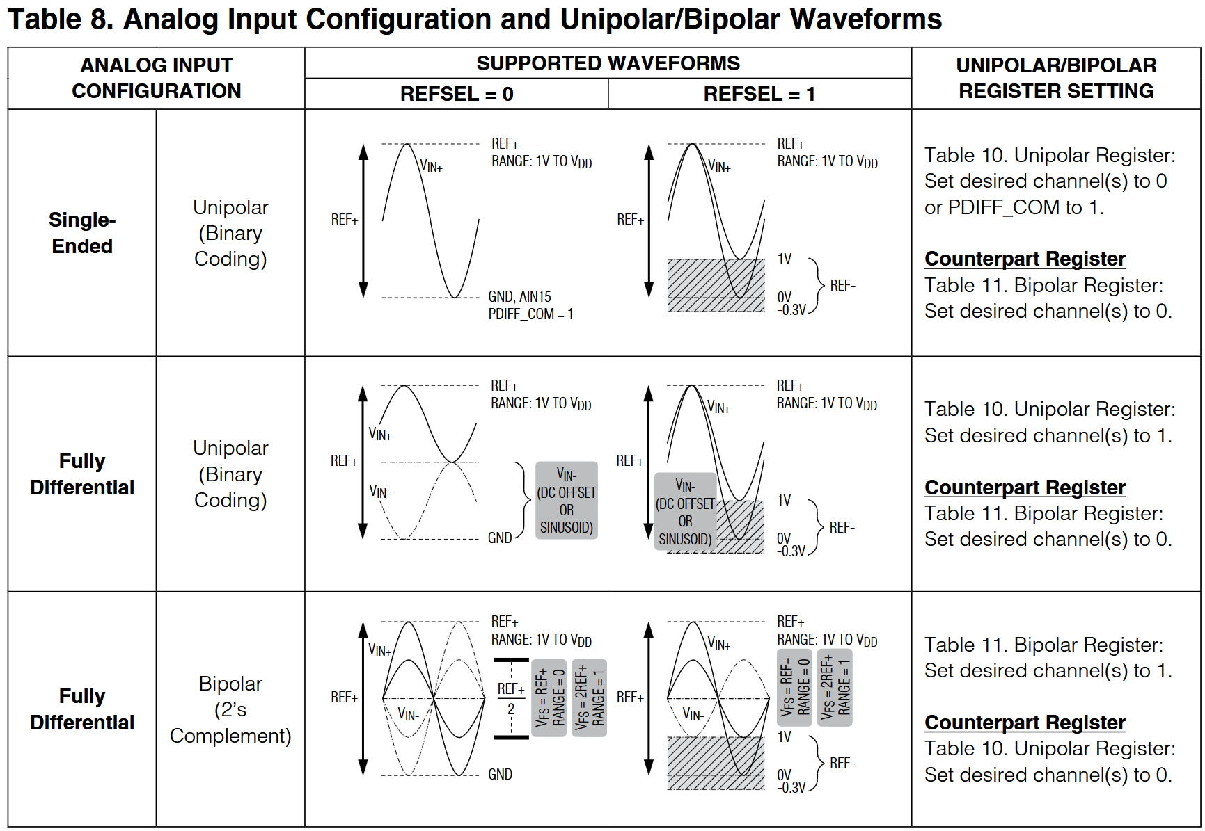
Fig. 501 Analog input configurations and waveforms, see Table 8 in [MAX11331_data_sheet]#
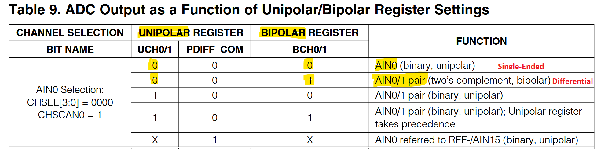
Fig. 502 Register configurations, see Table 9 in [MAX11331_data_sheet]#
Differential#
In differential mode, the ip core configures all channels with the following register set, resulting in 8 differential inputs with an input range of ±Vref.
UNIPOLAR = 0BIPOLAR = 1RANGE = 1PDIFF_COM = 0
This configuration is used in the uz_a_max11331 adapter card for 1. Fully differential (bipolar) measurement .
Single-ended#
In differential mode, the ip core configures all channels with the following register set, resulting in 16 single-ended inputs (referenced to ground of the UltraZohm) with an input range of 0..Vref.
UNIPOLAR = 0BIPOLAR = 0RANGE = 1PDIFF_COM = 0
Note that the UNIPOLAR register takes precedence over the RANGE and BIPOLAR registers.
Software Driver#
Configuration Procedure#
The test bench function below displays an example of how to configure and use the IP core. In this example the hardware trigger in the FPGA is used but instead the continuous sampling can be used as well.
The following settings are set globally for each IP-Core instance and are valid for all three masters (all three ADC chips on one adapter board):
base_address
ip_clk_frequency_Hz
trigger mode (either PL triggered or continuous sampling)
cpha
cpol
adc_delay_offset
clk_div
The following settings are set on a per channel basis within an IP-Core instance:
conversion_factor
offset
Example initialization of three IP-Core driver instances:
 #define XPAR_A3_ADC_MAX11331_IP_CORE_FREQUENCY 100000000U
 #define DEFAULT_MAX11331_CONVERSION_FACTOR 1.0f
 #define DEFAULT_MAX11331_INTEGER_BITS 14
 #define DEFAULT_MAX11331_FRACTIONAL_BITS 4
 #define DEFAULT_MAX11331_OFFSET 0

 void uz_adcMax11331_ip_core_init(void)
 {
     //Parameter set for one MAX11331 chip, thus one master
     struct uz_adcMax11331_config_t default_configuration = {
         .base_address = XPAR_UZ_ANALOG_ADAPTER_A3_ADAPTER_ADC_MAX11331_A3_BASEADDR,
         .ip_clk_frequency_Hz = XPAR_A3_ADC_MAX11331_IP_CORE_FREQUENCY,
         .channel_config = {
             .conversion_factor = DEFAULT_MAX11331_CONVERSION_FACTOR,
             .conversion_factor_definition = {
                 .is_signed = true,
                 .integer_bits = DEFAULT_MAX11331_INTEGER_BITS,
                 .fractional_bits = DEFAULT_MAX11331_FRACTIONAL_BITS},
             .offset = DEFAULT_MAX11331_OFFSET,
         },
         .trigger_mode=pl_trigger,
         .cpol = 1U,
         .cpha = 1U,
         .master_select = UZ_ADCMAX11331_MASTER1 | UZ_ADCMAX11331_MASTER2  | UZ_ADCMAX11331_MASTER3,
         .adc_delay_offset = 0,
                 .clk_div = UZ_ADCMAX11331_SPI_CLK_16_67MHZ};

         //1.) Create the instance of the first Max11331 adapter card with one or may several master = several physical Max11331 chips
     uz_adcMax11331_t *instance_1 = uz_adcMax11331_init(default_configuration);

     // Apply same configuration to all following instances, despite the base address of the FPGA IP Core
     //2.) Create the instance of the second Max11331 adapter board with one or may several master = several physical Max11331 chips
     default_configuration.base_address = XPAR_UZ_ANALOG_ADAPTER_A1_ADAPTER_A1_ADC_MAX11331_BASEADDR;
     uz_adcMax11331_t *instance_2 = uz_adcMax11331_init(default_configuration);
         //3.) Create the instance of the third Max11331 adapter board with one or may several master = several physical Max11331 chips
     default_configuration.base_address = XPAR_UZ_ANALOG_ADAPTER_A2_ADAPTER_A2_ADC_MAX11331_BASEADDR;
     uz_adcMax11331_t *instance_3 = uz_adcMax11331_init(default_configuration);
 }
Warning
The software driver has no way to read the trigger ADC signal enable_measure nor the output valid signal new_data! Thus, the user has to be sure that a ADC conversion took place and is finished. This means that the driver can mostly be used for debugging control algorithms that are fully implemented in the PL!
Driver reference#
-
typedef struct uz_adcMax11331_t uz_adcMax11331_t#
Data type for object adcMax11331.
-
struct uz_adcMax11331_config_t#
Configuration struct for adcMax11331.
Public Members
-
uint32_t base_address#
Base address of the IP-Core. No get or set function available
-
uint32_t ip_clk_frequency_Hz#
Clock frequency of the IP-Core. No get or set function available
-
uint32_t master_select#
One hot encoded variable to select the SPI masters that shall be configured. This corresponds to the physical ADC chip. 1 is the first chip, 2 the second chip, … The original UZ adapter board has e.g. 3 ADC chips The board from Chile has e.g. 6 ADC chips.
-
uint32_t adc_delay_offset#
Offset defined in number of clock cycles. It defines the delay between channel sampling. As more cycles, as longer the ADC waits until the next channel is sampled.
-
uint32_t clk_div#
See the SPI configuration register for explanation
-
uint32_t cpha#
SPI CPHA. Must be set to 1 for the Max11331
-
uint32_t cpol#
SPI CPOL. Must be set to 1 for the Max11331
-
uint32_t error_code#
One-Hot encoded error variable
-
uint32_t base_address#
-
uz_adcMax11331_t *uz_adcMax11331_init(struct uz_adcMax11331_config_t config)#
Initializes an instance of the adcMax11331.
This function allocates an instance of the IP core and updates the operation parameters that are shipped with the given uz_adcMax11331_config_t configuration struct
The function initializes the hardware by executing the following functions:
- Parameters:
config – Configuration values for the IP-Core
- Returns:
Pointer to initialized instance
-
void uz_adcMax11331_set_clk_div(uz_adcMax11331_t *self, uint32_t value)#
Asserts that not to many MSBs are set and that the value fits in the config register.
- Parameters:
self – Pointer to driver instance
value – Clock divider to scale the SCLK signal
-
void uz_adcMax11331_check_echo_of_master(uz_adcMax11331_t *self)#
Select the master from which the error status is read.
- Parameters:
self – Pointer to driver instance
Configuration Registers#
Status Register#
Address offset: 0x0
Software status register of the IP core.
Bit(s) |
Name |
Default Value |
Access |
Description |
|---|---|---|---|---|
0 |
Init_done |
0 |
Read |
A high flag gives feedback if the initialization is done. |
8 |
Meas_done |
0 |
Read |
A high flag gives feedback if the measurement is done. |
16 |
error |
0 |
Read |
A high flag gives feedback if an error is present. |
Error Counter Register#
Address offset: 0x04
Echoed bipolar 12 Register#
Address offset: 0x08
Read: Data sent by ADC connected to MISO, corresponding to echo of bipolar register value 1 and 2
Echoed bipolar 34 Register#
Address offset: 0x0C
Read: Data sent by ADC connected to MISO, corresponding to echo of bipolar register value 3 and 4
Echoed bipolar 56 Register#
Address offset: 0x10
Read: Data sent by ADC connected to MISO, corresponding to echo of bipolar register value 5 and 6
Echoed unibipolar 12 Register#
Address offset: 0x14
Read: Data sent by ADC connected to MISO, corresponding to echo of unipolar register value 1 and 2
Echoed unibipolar 34 Register#
Address offset: 0x18
Read: Data sent by ADC connected to MISO, corresponding to echo of unipolar register value 3 and 4
Echoed unibipolar 56 Register#
Address offset: 0x1C
Read: Data sent by ADC connected to MISO, corresponding to echo of unipolar register value 5 and 6
ADC Selector ForceInit Register#
Address offset: 0x20
Software ADC selector and force init register of the IP core.
Bit(s) |
Name |
Default Value |
Description |
|
|---|---|---|---|---|
5-0 |
Adc_selector |
0 |
Read/Write |
The LSB corresponds to the ADC which is connected to MISO 0 and MSB corresponds to the ADC which is connected to MISO 5. Set the bit to 1 to compare the sent init register with the echo register to verify the SPI communication of those ADCs. |
8 |
Force_init |
0 |
Read/Write |
Set to 1 to force 1 iteration of the init and then pass to the idle state even if SPI communication errors are found. |
CLK Division Register#
Address offset: 0x24
Software CLK division register of the IP core.
Bit(s) |
Name |
Default Value |
Access |
Description |
|---|---|---|---|---|
3-0 |
clk_division |
0 |
Read/Write |
The SPI sclk is generated internally by using a clock divider. The divider can be parameterized by the R5 processor. Clock divider 1 set the SPI SCK to 50Mhz. Divider 2 to 25Mhz. Divider 3 to 16.6Mhz and so on. The SPI SCK frequency will be given by: IP-Core clk frequency / (2 up (clock divider)). |
Vivado#
The only tested clock frequency for clk and s_axi_lite_aclk is 100 Mhz.
Port Name, CLK, Usage |
||
|---|---|---|
s_axi_lite |
100 MHz |
Slave AXI Lite bus to communicate with PS. Connect to AXI_smartconnect. |
clk |
100 MHz |
IP-core general clock. It should be connected to 100 MHz. |
reset_n |
100 MHz |
Active low reset. Reset the IP Core and its registers. When set to 1 the ip-core automatically start the initialization of ADC chips. Connect to 100 MHz reset. |
s_axi_lite_aclk |
100 MHz |
Slave AXI Lite clock. Connect to clk of 100 MHz. |
s_axi_lite_aresetn |
100 MHz |
Active low reset for Slave AXI Lite module. Connect to reset_n. |
Further information#
The state machine inside the IP-Core does not have a graph, however is easy to follow reading the VHDL code of the IP-Core.
References#
MAX11331 Adapter Card uz_a_max11331
Designed by#
Eyke Aufderheide (TUM), Sebastian Wendel (ZC) in 11/2024