R5 interrupts#
Software User Model#
The interrupt triggers the ISR_Control function (in isr.c) and the ADC conversion in the PL.
Four defines in uz_global_configuration.h control how the ISR and the ADC conversion are triggered:
INTERRUPT_ISR_SOURCE_USER_CHOICEselects the PWM counter event as the base trigger source.INTERRUPT_ISR_TRIGGER_ON_ADC_DATA_READYselects the ISR trigger mode:0: ISR triggers on the PWM event selected byINTERRUPT_ISR_SOURCE_USER_CHOICE. This results in a race condition between ADC data transfer and ISR execution.1: ISR triggers onaxi2tcm_write_done, i.e. after the ADC conversion is complete and the data has been transferred to TCM (~:math:1.3 mu s delay after the PWM event). This eliminates the race condition between ADC data transfer and ISR execution.
INTERRUPT_ADC_TO_ISR_RATIO_USER_CHOICEthe ADC is triggered every PWM event, butISR_Controlfires only every N-th event. See Mux Axi / ISR Trigger Control for details.ADC_TRIGGER_DELAY_IN_USadds an optional delay to the ADC trigger path. See Mux Axi / ISR Trigger Control for details.
// Select the PWM counter event used as the base trigger source:
#define INTERRUPT_ISR_SOURCE_USER_CHOICE        0U
// Trigger the ISR on axi2tcm_write_done instead of directly on the PWM event:
#define INTERRUPT_ISR_TRIGGER_ON_ADC_DATA_READY 1U
// Trigger the ADC every PWM event, but fire ISR_Control only every N-th:
#define INTERRUPT_ADC_TO_ISR_RATIO_USER_CHOICE  1U
// Optional delay added to the ADC trigger path (in microseconds):
#define ADC_TRIGGER_DELAY_IN_US                 0.0f
# |
Define name |
Interrupt trigger |
|---|---|---|
0 |
Interrupt_2L_max_min |
Two-Level PWM Module at minimum and maximum value of the triangular carrier |
1 |
Interrupt_2L_min |
Two-Level PWM Module at minimum value of the triangular carrier |
2 |
Interrupt_2L_max |
Two-Level PWM Module at maximum value of the triangular carrier |
3 |
Interrupt_3L_start_center |
Three-Level PWM Module at minimum and maximum value of the triangular carrier |
4 |
Interrupt_3L_start |
Three-Level PWM Module at minimum value of the triangular carrier |
5 |
Interrupt_3L_center |
Three-Level PWM Module at maximum value of the triangular carrier |
Note
When one of the two-level PWM sources is selected, update
uz_PWM_SS_2L_config_t.trigger_source in the PWM driver at the same time:
Interrupt_2L_minwithtrigger_at_MINInterrupt_2L_maxwithtrigger_at_MAXInterrupt_2L_max_minwithtrigger_at_EITHER
This keeps PWM register updates, ADC triggering, and ISR_Control
synchronized to the same carrier event.
Structure of the Interrupt#
        graph TB
    PWM_2L --> B[interrupts_in]
    PWM_3L --> B
    VIO --> B
    ATW(axi2tcm_write_done) --> B
    B --> mux_axi
    mux_axi -->|"interrupt_out_adc INTERRUPT_ISR_SOURCE"| delay_trigger
    mux_axi -->|"interrupt_out_isr INTERRUPT_ADC_TO_ISR_RATIO"| IV[Interrupt_vector]
    delay_trigger -->|"ADC_TRIGGER_DELAY_IN_US"| ADC_conversion
    ADC_conversion --> ATW
    ATW --> IV
    IV -->|"INTERRUPT_ISR_TRIGGER_ON_ADC_DATA_READY"| ISR_Control
Fig. 59 Signal flow in PL for ADC trigger and ISR trigger#
The Interrupt module consists of:
mux_axi: chooses the ADC conversion trigger source, the ADC-to-ISR ratio, and configures the ADC trigger delaydelay_trigger: adds the configured delay to the ADC conversion triggervio_interrupt: manually injects an interrupt trigger via Vivado hardware manager for debugging
From an outside perspective, the interrupt gets six different sources for the interrupt and outputs the selected signal to the PS interrupt and to trigger_conversions for the ADC.
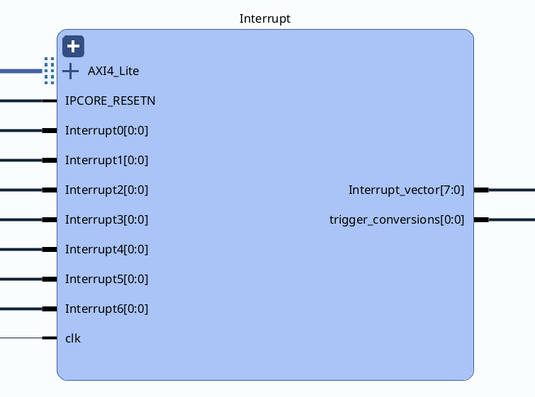
Fig. 60 Top view of the PL module of the interrupt structure. Interrupt6 is the signal from axi2tcm_write_done.#
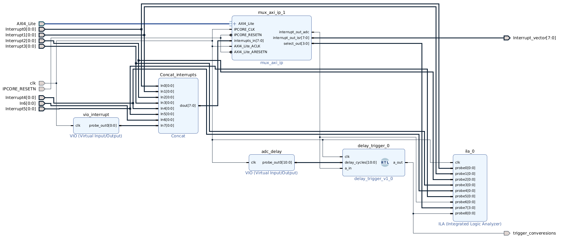
Fig. 61 PL module of the interrupt structure.#
In Vivado, the signals connected to pl_ps_irq0 are assigned an interrupt ID starting at XPS_FPGA0_INT_ID for bit 0 and increasing with each additional signal.
In our project, the Interrupt_vector is directly connected to pl_ps_irq0.
With this logic, the interrupt IDs are assigned in isr.h.
Note that XPS_FPGAx_INT_ID is defined in xparameters_ps.h.
Trigger of ADC Conversion#
The ADC conversion is always triggered by the PWM source selected via INTERRUPT_ISR_SOURCE_USER_CHOICE, regardless of the ISR trigger mode set by INTERRUPT_ISR_TRIGGER_ON_ADC_DATA_READY.
In some applications, the ADC conversion needs to be delayed relative to the PWM trigger, for example when using IGBTs, where the switching transient must settle before sampling.
To prevent ADC sampling during a switching event, this delay can be added in PL via ADC_TRIGGER_DELAY_IN_US in uz_global_configuration.h.
The software driver converts the configured value in microseconds to clock cycles and rounds up to the next achievable step.
This delay applies in both ISR trigger modes: when INTERRUPT_ISR_TRIGGER_ON_ADC_DATA_READY = 1, the ISR fires after the (already delayed) ADC conversion completes and the data has been transferred to TCM.
For more details on the register and driver interface, see Mux Axi / ISR Trigger Control.
Delay Trigger Block#
The PL delay is implemented by delay_trigger.vhd in ip_cores/Delay_signal.
The block behavior is:
delay_cycles = 0routesa_indirectly toa_outdelay_cycles = 1..1023emits a delayed output pulse after the configured number ofclkcyclesthe output pulse width is fixed locally in the VHDL source via
pulse_width_cycles_cchanging
delay_cyclesclears any pending delayed triggera second rising edge while a delayed pulse is pending or active is ignored
pulse_pendingindicates that a delayed trigger is pending or currently being emitted
With the default 100 MHz clock used in the interrupt path, the achievable delay range is 0 to 10.23 us in 10 ns steps.
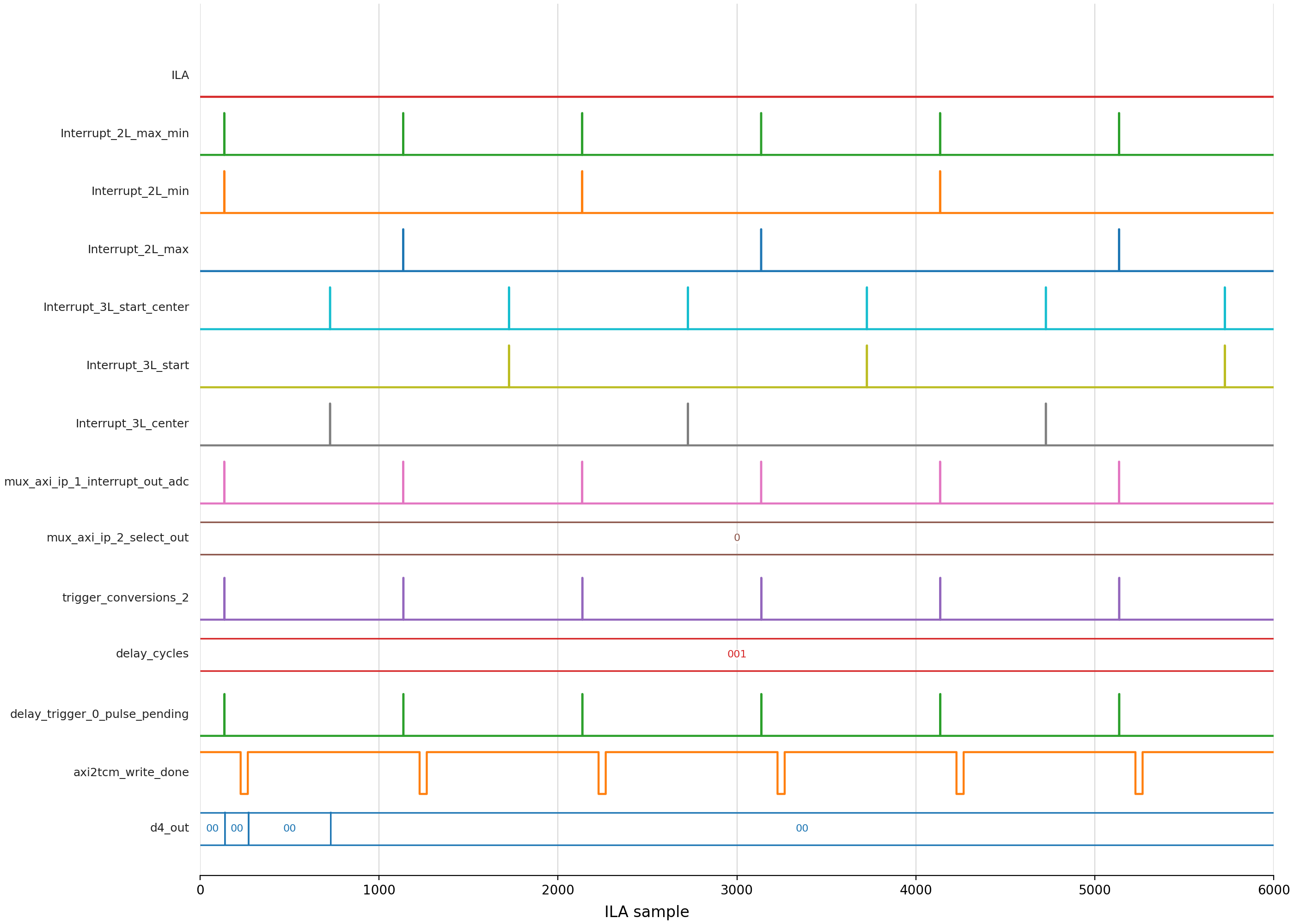
ILA Timing Example#
The following timing diagram is generated directly from interrupt_ila_data.csv and therefore stays in sync with the captured hardware data.
It plots all recorded CSV signals over the full capture range in one figure, without selecting a subset of traces or creating zoomed views.
(Source code, png, hires.png, pdf)
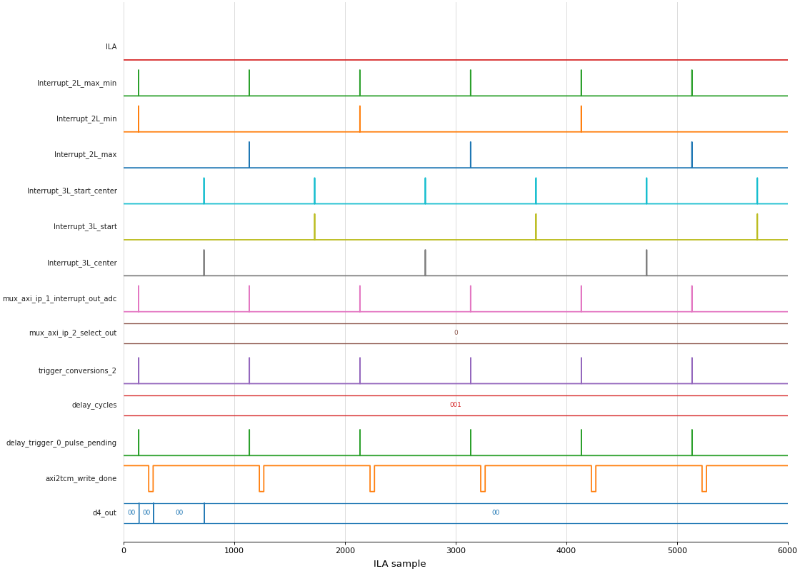
Fig. 62 Timing diagram generated from ILA export in interrupt_ila_data.csv.#