Constraints#
The constraints are used to assign I/O ports to physical pins of the MPSoC by setting the property PACKAGE_PIN.
Refer to the Xilinx documentation for more information about pin planning: Xilinx information.
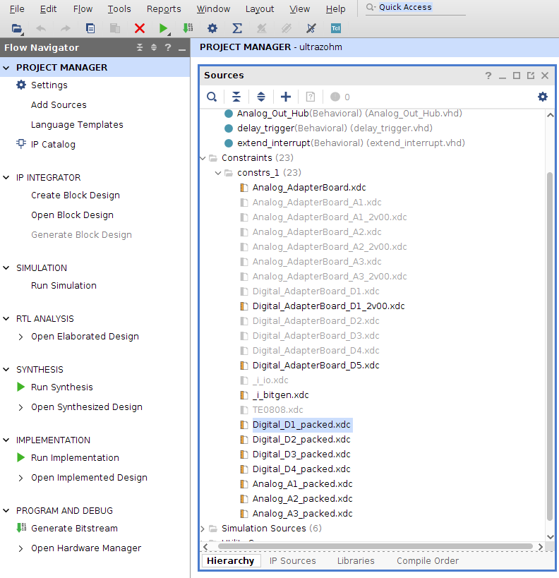
Fig. 34 Location of the constraint files.#
Note
There are disabled constraint files in the project. Only use them if you have a version 1v5 of the carrier board!
Usage#
The I/O constraints (pin planning) are not meant to be changed since the pins of the MPSoC are routed to the adapter cards. Use the output ports, e.g., D1_out if you want the signal of the PL to be routed to the digital adapter slot D1:
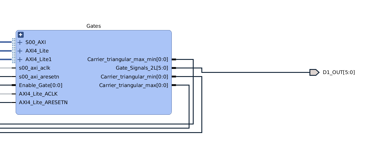
Fig. 35 I/O port D1_out[0..5]#
The following code maps the ports D1_out to the PINs.
set_property PACKAGE_PIN AC9    [get_ports D1_OUT[0]]
set_property PACKAGE_PIN AB9    [get_ports D1_OUT[1]]
set_property PACKAGE_PIN AB10   [get_ports D1_OUT[2]]
set_property PACKAGE_PIN AB11   [get_ports D1_OUT[3]]
set_property PACKAGE_PIN AJ11   [get_ports D1_OUT[4]]
set_property PACKAGE_PIN AK11   [get_ports D1_OUT[5]]
Schematic names#
The port name corresponds to the signal name in the carrier board schematic and is routed to the digital and analog adapter card slots D1..D5 (X6) and A1..A3 (X5).
Constraint |
1v5 |
v2 |
v3 |
v4 |
D1_OUT[0..29] |
DIG_01_Ch..DIG_30Ch |
DIG_01_Ch..DIG_30Ch |
DIG_01_Ch..DIG_30Ch |
D1[0..29] |
The I/O ports D1_OUT[0..5] are routed to D1.
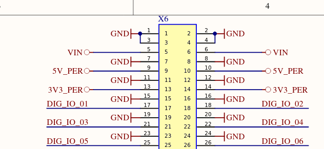
Fig. 36 I/O port D1_out[0..5] at X6 with DIG_IO_01.._06#
Default constraints of analog adapter cards A1, A2, A3#
The following table lists the mapping in the default Vivado project (see Global configuration) of the carrier board with the ADC IP core (ADC LTC2311 V3) and the ADC adapter card (Analog LTC2311-16 3v01).
Carrierboard schematic name |
FPGA pin name |
Vivado port name |
|---|---|---|
ANL_09_P |
AH9 |
A1_IN[0] |
ANL_09_N |
AJ9 |
A1_IN[1] |
ANL_07_P |
AH12 |
A1_IN[2] |
ANL_07_N |
AJ12 |
A1_IN[3] |
ANL_05_P |
AD5 |
A1_IN[4] |
ANL_05_N |
AE5 |
A1_IN[5] |
ANL_03_P |
AF11 |
A1_IN[6] |
ANL_03_N |
AG11 |
A1_IN[7] |
ANL_10_P |
AB6 |
A1_IN[8] |
ANL_10_N |
AB5 |
A1_IN[9] |
ANL_08_P |
AK13 |
A1_IN[10] |
ANL_08_N |
AK12 |
A1_IN[11] |
ANL_06_P |
AF8 |
A1_IN[12] |
ANL_06_N |
AF7 |
A1_IN[13] |
ANL_04_P |
AG13 |
A1_IN[14] |
ANL_04_N |
AH13 |
A1_IN[15] |
ANL_02_P |
AG10 |
A1_OUT_CNV_1[0] |
ANL_02_N |
AF10 |
A1_OUT_CNV_0[0] |
ANL_01_P |
AG8 |
A1_OUT_CLK[0] |
ANL_01_N |
AH8 |
A1_OUT_CLK[1] |
Carrierboard schematic name |
FPGA pin name |
Vivado port name |
|---|---|---|
ANL_09_P |
AB4 |
A2_IN[0] |
ANL_09_N |
AC4 |
A2_IN[1] |
ANL_07_P |
AJ5 |
A2_IN[2] |
ANL_07_N |
AK5 |
A2_IN[3] |
ANL_05_P |
AH3 |
A2_IN[4] |
ANL_05_N |
AH2 |
A2_IN[5] |
ANL_03_P |
AF6 |
A2_IN[6] |
ANL_03_N |
AF5 |
A2_IN[7] |
ANL_10_P |
AH6 |
A2_IN[8] |
ANL_10_N |
AJ6 |
A2_IN[9] |
ANL_08_P |
AH4 |
A2_IN[10] |
ANL_08_N |
AJ4 |
A2_IN[11] |
ANL_06_P |
AG6 |
A2_IN[12] |
ANL_06_N |
AG5 |
A2_IN[13] |
ANL_04_P |
AJ10 |
A2_IN[14] |
ANL_04_N |
AK10 |
A2_IN[15] |
ANL_02_P |
AK8 |
A2_OUT_CNV_1[0] |
ANL_02_N |
AK9 |
A2_OUT_CNV_0[0] |
ANL_01_P |
AH7 |
A2_OUT_CLK[0] |
ANL_01_N |
AJ7 |
A2_OUT_CLK[1] |
Carrierboard schematic name |
FPGA pin name |
Vivado port name |
|---|---|---|
ANL_09_P |
AD4 |
A3_IN[0] |
ANL_09_N |
AE4 |
A3_IN[1] |
ANL_07_P |
AF3 |
A3_IN[2] |
ANL_07_N |
AG3 |
A3_IN[3] |
ANL_05_P |
AK4 |
A3_IN[4] |
ANL_05_N |
AK3 |
A3_IN[5] |
ANL_03_P |
AK7 |
A3_IN[6] |
ANL_03_N |
AK6 |
A3_IN[7] |
ANL_10_P |
AC7 |
A3_IN[8] |
ANL_10_N |
AD7 |
A3_IN[9] |
ANL_08_P |
AG1 |
A3_IN[10] |
ANL_08_N |
AH1 |
A3_IN[11] |
ANL_06_P |
AC2 |
A3_IN[12] |
ANL_06_N |
AD2 |
A3_IN[13] |
ANL_04_P |
AE3 |
A3_IN[14] |
ANL_04_N |
AE2 |
A3_IN[15] |
ANL_02_P |
AK2 |
A3_OUT_CNV_1[0] |
ANL_02_N |
AJ2 |
A3_OUT_CNV_0[0] |
ANL_01_P |
AB8 |
A3_OUT_CLK[0] |
ANL_01_N |
AC8 |
A3_OUT_CLK[1] |