Analog LTC2311-16 3v01#
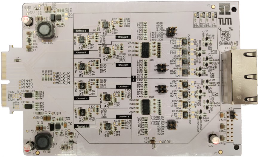
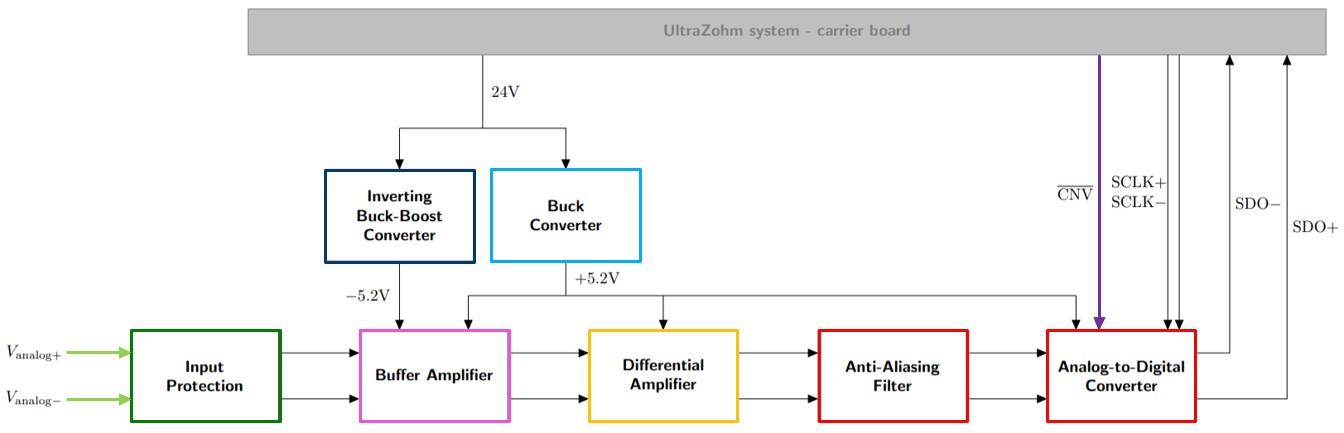
Diagrams#
Block diagram
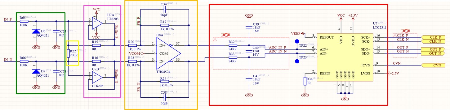
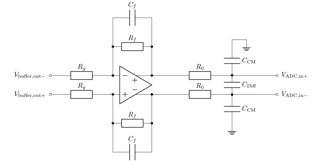
Schematic excerpt
PCB colored
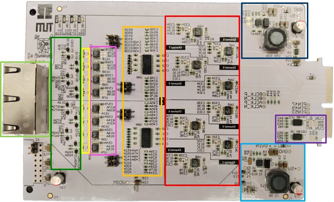
From left to right
Notice that the picture of the PCB is flipped to match the orientation of the block diagram and schematic.
Color |
Functionality |
|---|---|
light green |
Analog inputs on RJ45 |
dark green |
Input protection (ESD diodes) |
yellow |
Measurement shunt resistor (optional, not populated) |
pink |
Voltage follower to increase input impedance and avoid loading the sensor |
orange |
Differential OpAmp to scale and filter signals |
red |
Anti-aliasing filter and ADC |
dark blue |
Inverting buck-boost converter for -5V |
light blue |
Buck converter for +5V |
purple |
Buffer for CNV signal coming from the FPGA |
Filters#
The crossover frequency \(f_\mathrm{aliasing,-3dB}\) of the anti-aliasing filter (red) is formed by the capacitors \(C_\mathrm{Diff}\) and \(C_\mathrm{CM}\). They create a first order low-pass filter with the series resistors \({R_0}\) with
Additionally, \(C_\mathrm{f}\) and \(R_\mathrm{f}\) form an active first-order low-pass filter, with
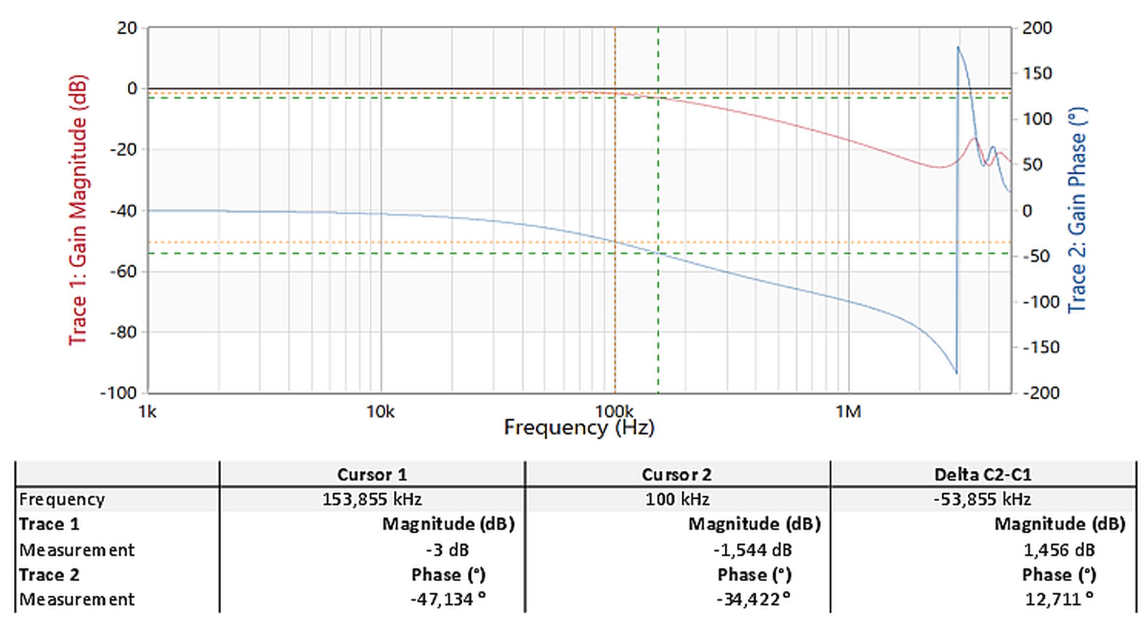
The resulting transfer function of the signal conditioning stage, i.e., from the RJ45 input connectors to the \(V_\mathrm{ADC,in}\) (including the buffer and filter stages up to the point where the signal enters the ADC), is measured with the Bode100. The resulting bode plot is depicted below.
Measurement accuracy#
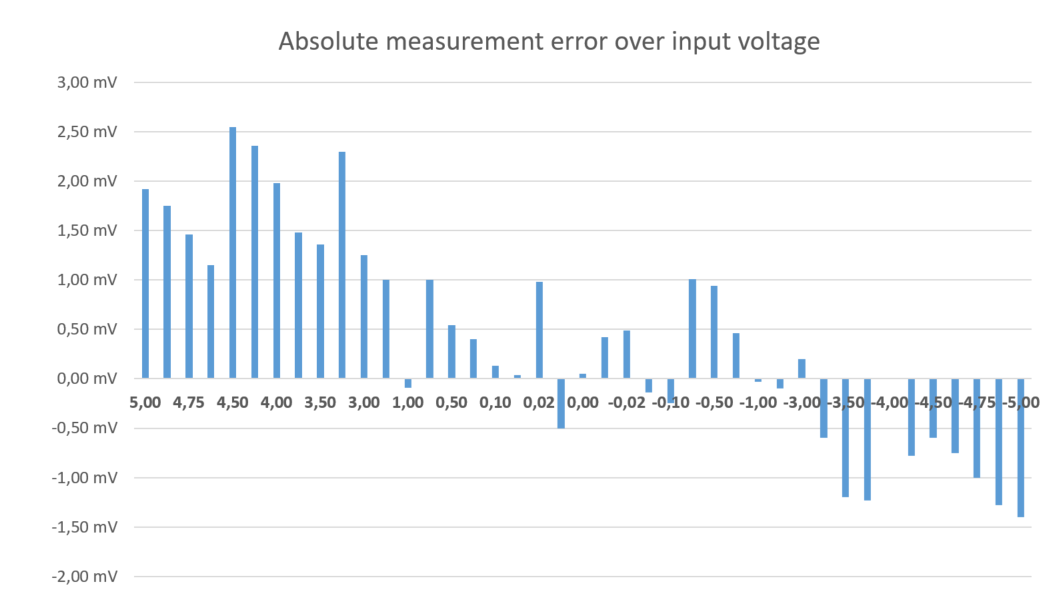
The signal conditioning stage of the adapter card is validated with a 6 1/2 digit multimeter yielding the following results. This suggests that a measurement error below 2mV can be expected over the full input range.
Adjust measurement gains#
For all types of measurements, described in Measurement modes, it is recommended to adjust the gains of the differential operational amplifier (orange) to utilize the full input range of the ADC, i.e., \({\pm 5}\) V. Initially, the gain is set to
Note
Use a high precision resistor to set the gains, i.e., 0.1% or better.
The pre-assembled values are
\({R_f}\) |
\({1\,\mathrm{k\Omega}}\) |
\({R_g}\) |
\({1\,\mathrm{k\Omega}}\) |
\({C_f}\) |
\({56\,\mathrm{pF}}\) |
\({R_0}\) |
\({24.9\,\mathrm{\Omega}}\) |
\({C_\mathrm{CM}}\) |
\({12\,\mathrm{nF}}\) |
\({C_\mathrm{Diff}}\) |
\({16\,\mathrm{nF}}\) |
Note
You can also use the LTSpice simulation to find the correct gains and filter values for your setup. The simulation files are attached at the end of this document.
Compatibility#
Slots A1 to A3 can be used without limitations
References#
See IP core ADC LTC2311 V3
Designed by#
Simon Lukas (TUM), Eyke Liegmann (TUM) in 09/2020