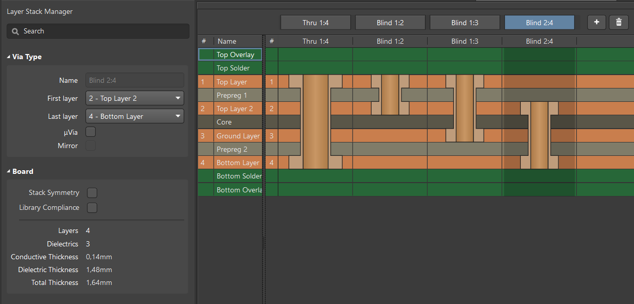
The layer stack manager defines the structure and the width of the different layers.
If the PCB should correspond to “standard” layer stack structure the best way would be to use the described and given layer stack recommendations of the PCB manufacturer.
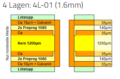
In the following the layer stack for the manufacturer MultiCB is used:
Different via types are possible to use.
As well as by the layer stack the possibility of using different vias types is depending on the PCB manufacturer.
Because of that, the kind and size of vias that should be used in the project must be checked with the capabilities of the manufacturer.
As general rule use only through-hole vias that drill from top to bottom, everything else is more expensive.
Open the layer stack manager (only possible if you select a PCB Document “.PcbDoc”) by clicking Design –> LayerStackManager
Choose the register “Via types” (Below the layer stack table)
Configure the types of possible via types for this project (through hole vias, blind vias or buried vias)