Analog LTC2311-16 Rev05 and Rev06#
Changes compared to the previous version#
switched to single-channel differential op-amp THS4561
negative rail of differential op-amp THS4561 is supplied with small negative voltage to allow true voltage swing from 0 to 5V driving the ADC
adapted filter design for higher frequency to avoid the influence of kick-back voltage at high sampling rates
power rails are generated from LDOs
For Rev06: Due to chip shortage, the LMK1C1104 is not available. Therefore it was replaced by the LMK1C1108 which distributes the conversion signal (CNV) to all eight ADCs. Besides this, it is identical to Rev05.
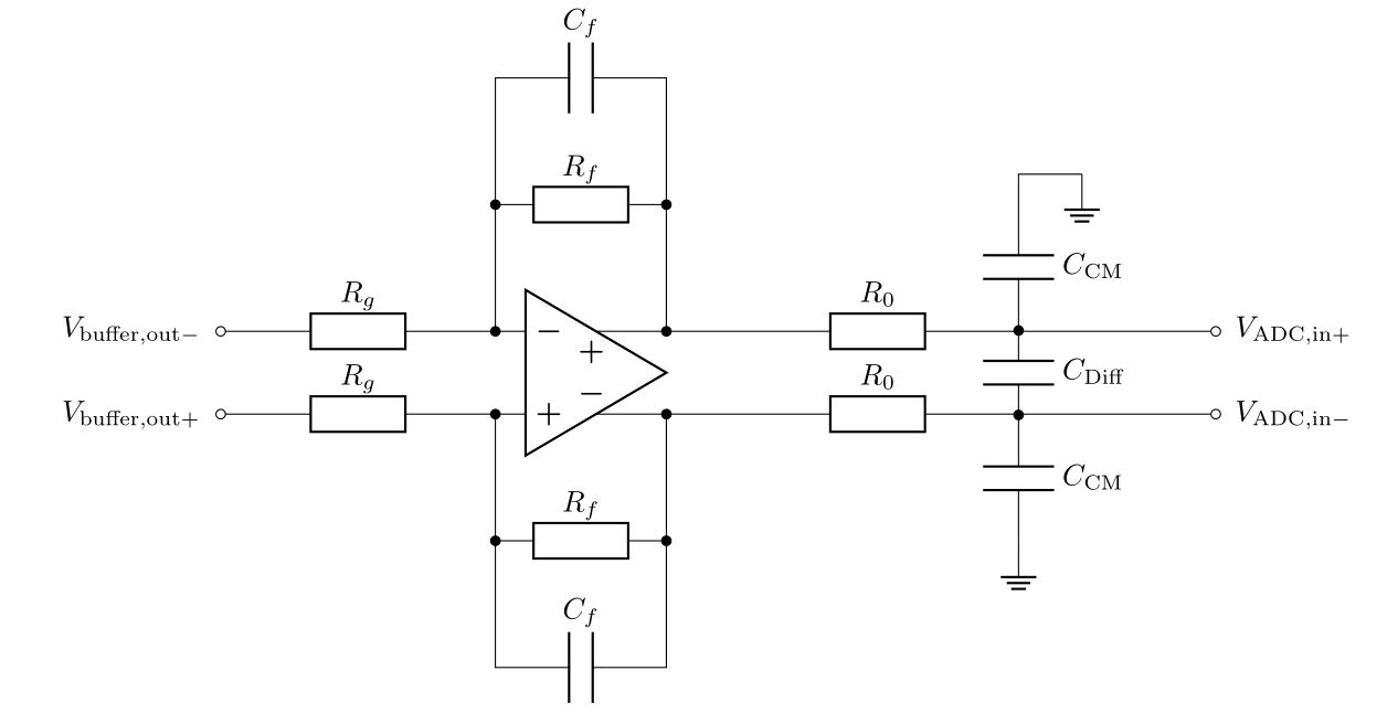
Filters#
1. The crossover frequency \(f_\mathrm{aliasing,-3dB}\) of the anti-aliasing filter is formed by the capacitors \(C_\mathrm{Diff}\) and \(C_\mathrm{CM}\). They create a first-order low-pass filter with the series resistors \({R_0}\) with
Additionally, \(C_\mathrm{f}\) and \(R_\mathrm{f}\) form an active first-order low-pass filter, with
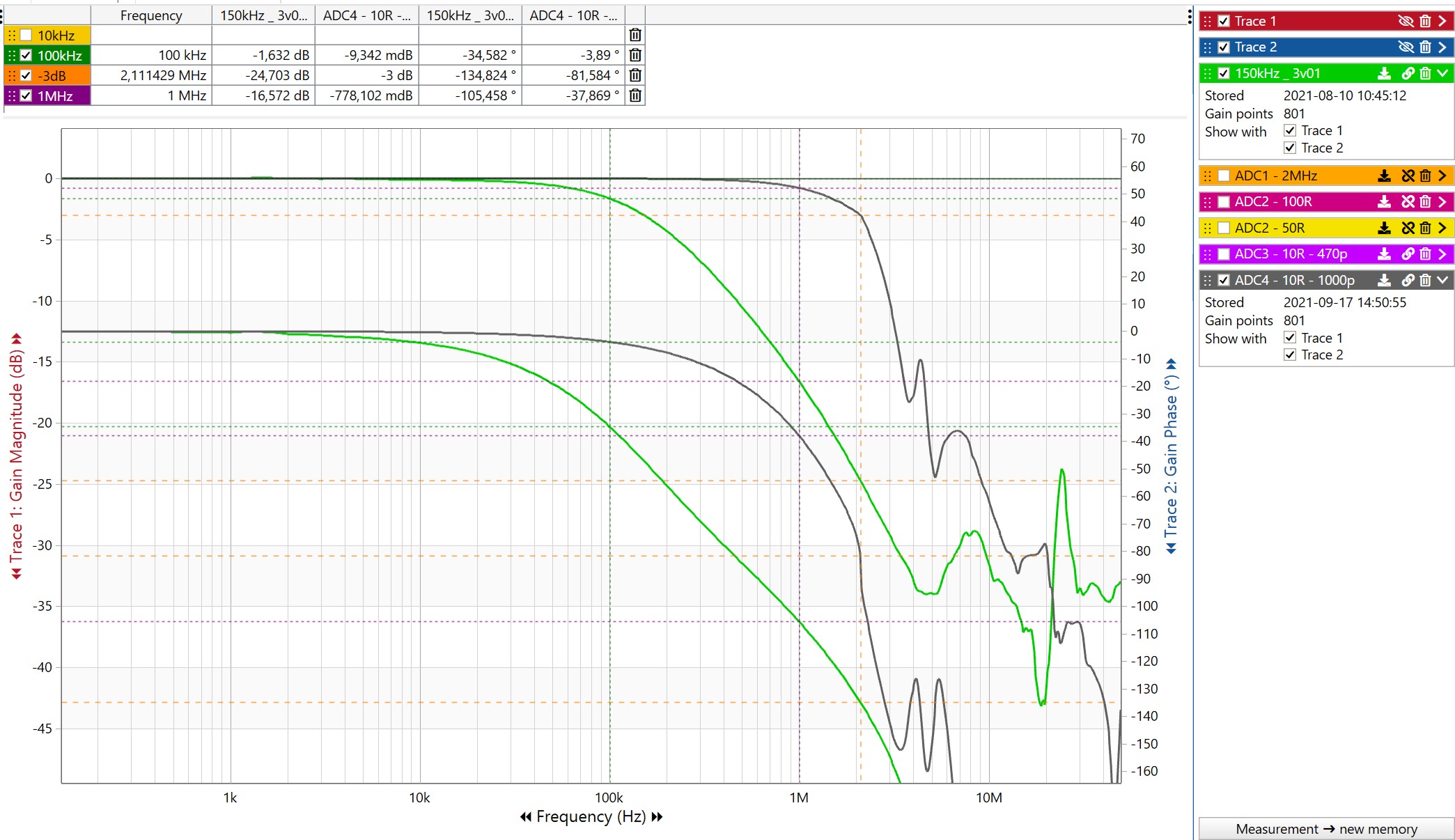
The resulting transfer function of the signal conditioning stage, i.e., from the RJ45 input connectors to the \(V_\mathrm{ADC,in}\) (including the buffer and filter stages up to the point where the signal enters the ADC), is measured with the Bode100. The resulting bode plot is depicted below.
Adjust measurement gains#
For all types of measurements, described in Measurement modes, it is recommended to adjust the gains of the differential operational amplifier to utilize the full input range of the ADC, i.e., \({\pm 5}\) V. Initially, the gain is set to
Note
Use a high precision resistor to set the gains, i.e., 0.1% or better.
The pre-assembled values are
\({R_f}\) |
\({1\,\mathrm{k\Omega}}\) |
\({R_g}\) |
\({1\,\mathrm{k\Omega}}\) |
\({C_f}\) |
\({56\,\mathrm{pF}}\) |
\({R_0}\) |
\({10\,\mathrm{\Omega}}\) |
\({C_\mathrm{CM}}\) |
\({1\,\mathrm{nF}}\) |
\({C_\mathrm{Diff}}\) |
\({1\,\mathrm{nF}}\) |
Note
You can also use the LTSpice simulation to find the correct gains and filter values for your setup. The simulation files are attached at the end of this document.
Compatibility#
Slots A1 to A3 can be used without limitations
References#
See IP core ADC LTC2311 V3
Designed by#
Eyke Liegmann (TUM) in 09/2021