Loopback PCB#
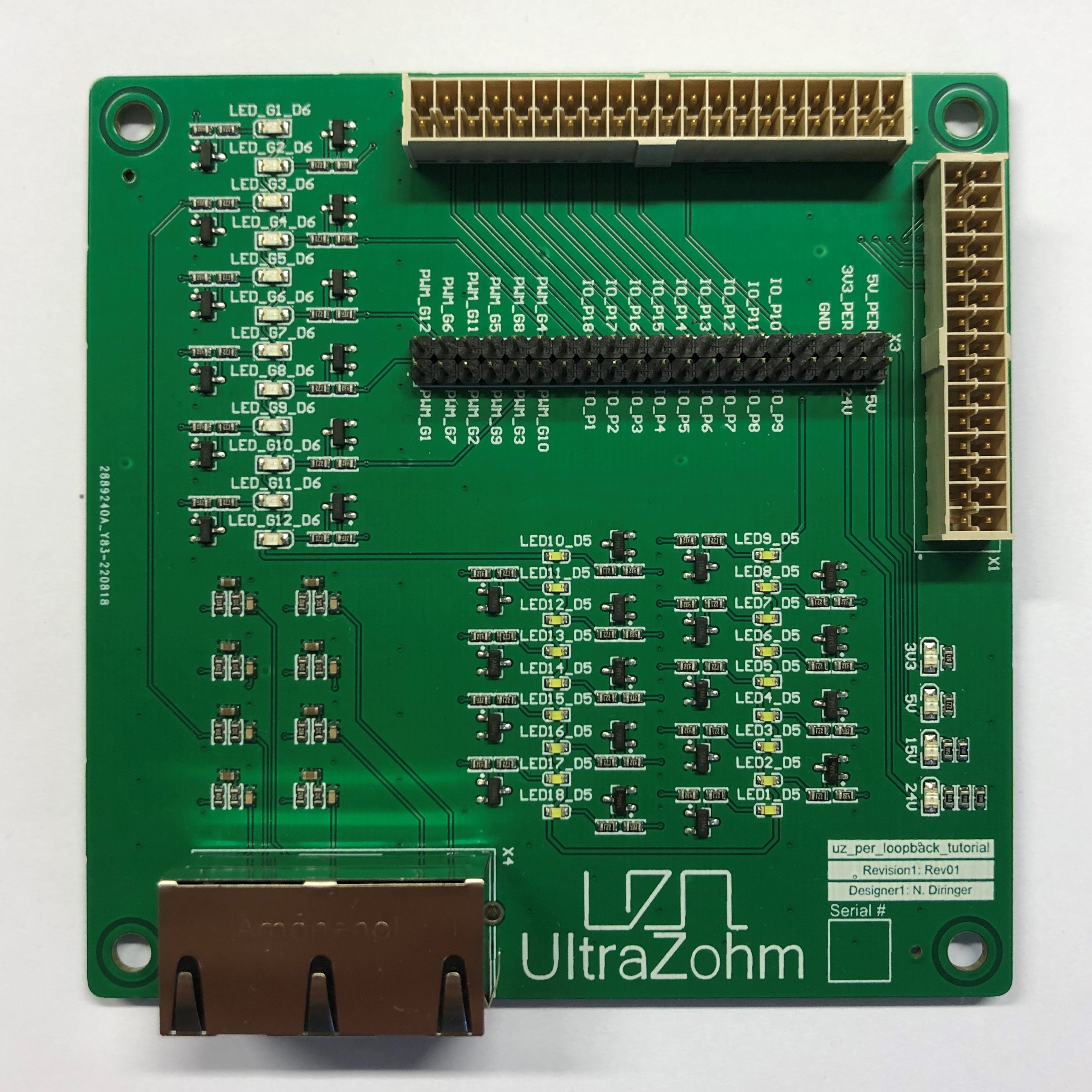
Fig. 284 Loopback PCB#
Source#
Revisions#
Rev01
General description#
This PCB is part of the ADC Loopback tutorial.
The LEDs indicate the state of the signals from the digital voltage card (Digital Voltage 3U 2v01). Furthermore eight of the signals (as documented in the section Signal description below) are first filtered and then output via the Ethernet connector to the ADC card (Analog LTC2311-16 3v01, Analog LTC2311-16 2vXX ).
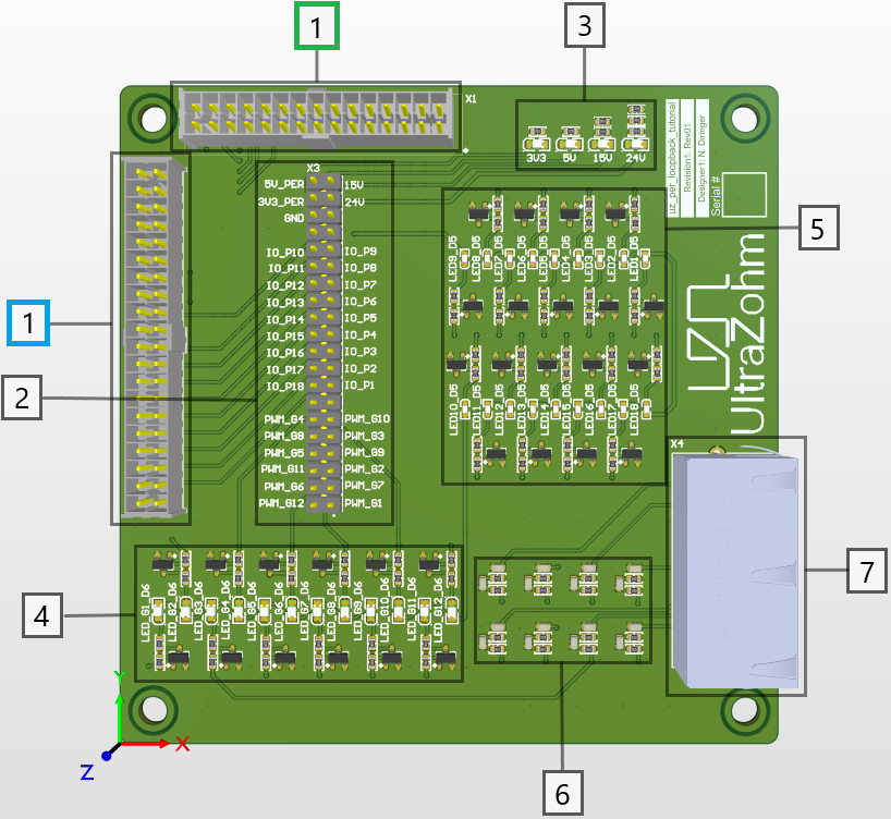
Fig. 285 Functional areas of the Loopback PCB#
Layout#
The PCB is structured by functional areas as shown in the Fig. 285 on the right.
Connectors to the Digital Voltage Card
Connector 1: IPL1-115-01-L-D-K, top (green)
Connector 2: IPL1-120-01-L-D-K, left (blue)
Pin header for measuring all signals
Supply voltage state indicated by LEDs (3V3, 5V, 15V, 24V)
State of gate signals indicated by LEDs
State of remaining I/Os indicated by LEDs
Low pass filter for filtering the gate signals
Ethernet connector to ADC Card
Signal description#
Since the matching of the signal names between the PCBs used in the Loopback Tutorial is not intuitive, the following table matches the signal names of the Digital Voltage Card to the signal names on the Loopback PCB and the ADC card. Additionally, the name of the corresponding LED as marked on the Loopback PCB is given.
Connector 1: IPL1-115-01-L-D-K#
Pin |
Digital voltage card |
Loopback PCB |
LED |
ADC card |
|---|---|---|---|---|
1 |
VIN |
24V |
24V |
|
2 |
DIG_IO_P1 |
PWM_G1 |
LED_G1_D6 |
AIN_A_P4 |
3 |
DIG_IO_P2 |
PWM_G7 |
LED_G7_D6 |
AIN_B_P2 |
4 |
DIG_IO_P3 |
PWM_G2 |
LED_G2_D6 |
AIN_A_P3 |
5 |
DIG_IO_P4 |
PWM_G9 |
LED_G9_D6 |
|
6 |
DIG_IO_P5 |
PWM_G3 |
LED_G3_D6 |
AIN_A_P2 |
7 |
DIG_IO_P6 |
PWM_G10 |
LED_G10_D6 |
|
8 |
DIG_IO_P7 |
IO_P1 |
LED1_D5 |
|
9 |
DIG_IO_P8 |
IO_P2 |
LED2_D5 |
|
10 |
15V |
15V |
15V |
|
11 |
DIG_IO_P9 |
IO_P3 |
LED3_D5 |
|
12 |
DIG_IO_P10 |
IO_P4 |
LED4_D5 |
|
13 |
DIG_IO_P11 |
IO_P5 |
LED5_D5 |
|
14 |
DIG_IO_P12 |
IO_P6 |
LED6_D5 |
|
15 |
DIG_IO_P13 |
IO_P7 |
LED7_D5 |
Fig. 286 Netnames of connector 1 (IPL1-115-01-L-D-K) on Digital voltage card#
Fig. 287 Netnames of connector 1 (IPL1-115-01-L-D-K) on Loopback PCB#
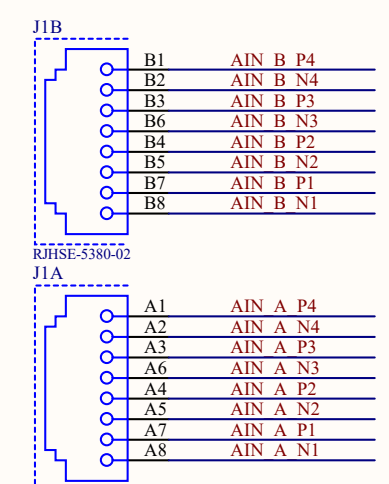
Fig. 288 Netnames of Ethernet connector on ADC card#
Connector 2: IPL1-120-01-L-D-K#
Pin |
Digital voltage card |
Loopback PCB |
LED |
ADC card |
|---|---|---|---|---|
1 |
VIN |
24V |
24V |
|
2 |
DIG_IO_P14 |
PWM_G4 |
LED_G4_D6 |
AIN_A_P1 |
3 |
DIG_IO_P15 |
PWM_G8 |
LED_G8_D6 |
AIN_B_P1 |
4 |
DIG_IO_P16 |
PWM_G5 |
LED_G5_D6 |
AIN_B_P4 |
5 |
DIG_IO_P17 |
PWM_G11 |
LED_G11_D6 |
|
6 |
DIG_IO_P18 |
PWM_G6 |
LED_G6_D6 |
AIN_B_P3 |
7 |
DIG_IO_P19 |
PWM_G12 |
LED_G12_D6 |
|
8 |
DIG_IO_P20 |
IO_P8 |
LED8_D5 |
|
9 |
DIG_IO_P21 |
IO_P9 |
LED9_D5 |
|
10 |
3V3 |
3V3 |
3V3 |
|
11 |
DIG_IO_P22 |
IO_P10 |
LED10_D5 |
|
12 |
DIG_IO_P23 |
IO_P11 |
LED11_D5 |
|
13 |
DIG_IO_P24 |
IO_P12 |
LED12_D5 |
|
14 |
DIG_IO_P25 |
IO_P13 |
LED13_D5 |
|
15 |
DIG_IO_P26 |
IO_P14 |
LED14_D5 |
|
16 |
DIG_IO_P27 |
IO_P15 |
LED15_D5 |
|
17 |
DIG_IO_P28 |
IO_P16 |
LED16_D5 |
|
18 |
DIG_IO_P29 |
IO_P17 |
LED17_D5 |
|
19 |
DIG_IO_P30 |
IO_P18 |
LED18_D5 |
|
20 |
5V |
5V |
5V |
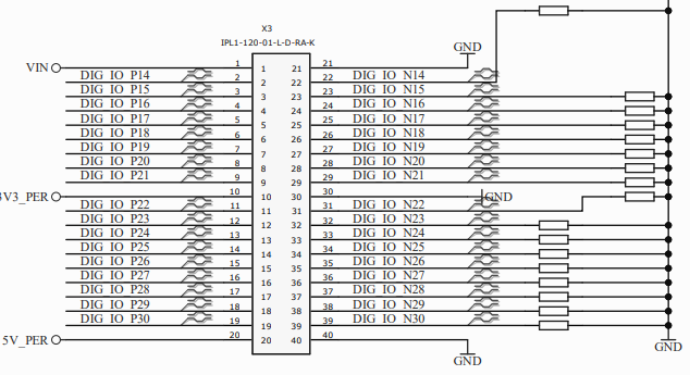
Fig. 289 Netnames of connector 2 (IPL1-120-01-L-D-K) on Digital voltage card#
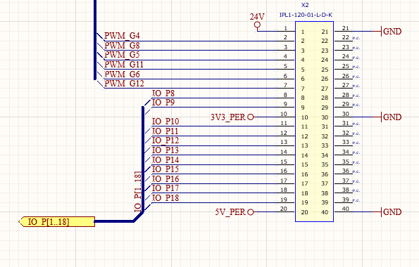
Fig. 290 Netnames of connector 2 (IPL1-120-01-L-D-K) on Loopback PCB#
Fig. 291 Netnames of Ethernet connector on ADC card#
Hint
To sum this up: The signals on Pin 2 to Pin 7 on both connectors (IPL1-115-01-L-D-K & IPL1-120-01-L-D-K) are used for the gate signals in the Loopback tutorial. P2 being the gate signal for the first high side switch, P3 for the corresponding low side switch, P4 for the second high side switch and so on. All Gate signals for the high side switches (Pin 2, Pin 4, Pin 6) and the first for the low side switches (Pin 3) are filtered and can be read back by the ADC card.
Downloads#
Rev01
Designer#
Designed by Nina Diringer (TH Nürnberg), 07/2022