uz_dac8831#
The DAC card features 8 independent, 16-bit digital analog conversion channels with one DAC8831 for each channel. The DAC8831 has a settling time of \(1~\mu s\) according to the data sheet which leads to a maximum frequency of \(1 MHz\) for changing the output voltage (not tested!). The SPI interface of the DAC8831 has a maximum clock frequency of \(50 MHz\), which is tested and working on the adapter card. The output voltage is bipolar with a range of +-5V (differential). Each DAC8831 is connected to an individual data channel and all 8 DAC8831 share the chip select (CS) as well as the clock (CLK) of the SPI interface. The DAC8831 features an LDAC pin that determines when new set-points are applied to the output. This pin is not used in the design (pulled up). Therefore, all ADC channels change their set-point according to the data they receive with each rising edge on the CS signal (all channels simultaneously).
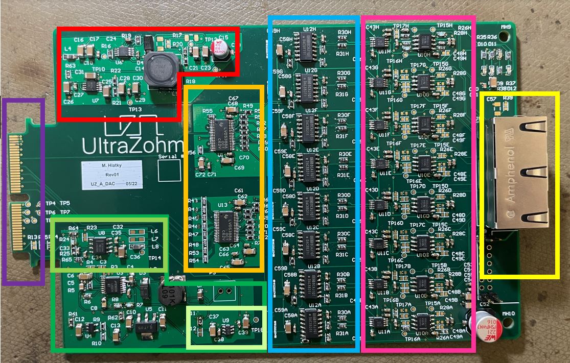
Fig. 238 Assembled DAC PCB with power supply and reference voltage (red and green), LVDS receiver (orange), DAC8831 (blue), output OpAMPs (pink), loopback connection (purple) and Ethernet connector (yellow).#
The output of the DAC card is fully compatible to Analog LTC2311-16, i.e., it can directly connect to the card with matching voltage levels and DAC1 corresponds to ADC1 on channel A. Fig. 239 shows the typical application of the DAC card. The DAC card is used to loop values from the FPGA through the ADC card back to the FPGA. This setup enables HIL testing including the whole signal chain of the ADC.
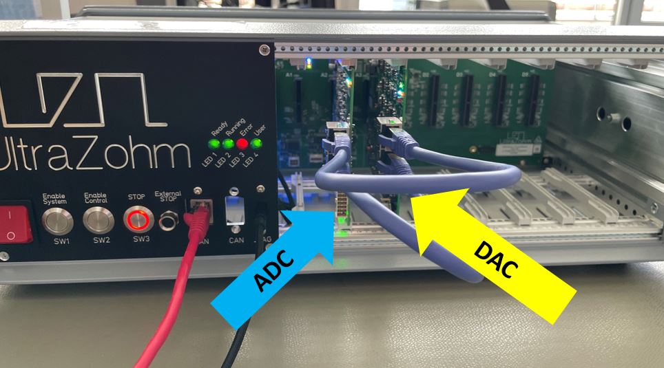
Fig. 239 Typical application of the DAC card in loopback operation with Analog LTC2311-16.#
Measurements#
The following measurements are conducted using the loopback configuration of Fig. 239 and the uz_dac_spi_interface IP core. The software writes the values for the DAC output from the Waveform Generator to the IP core in each ISR while the ADC reads the values. Therefore, a delay between write to the DAC and the measurement of the ADC of one interrupt sample time is present. Additionally, the ADC always measures the signal of the DAC after the settling time has passed due to the timing of the system. Thus, the overshoot and settling of the DAC output is not present in the measurement logs in loopback operation.
Note that the DAC card features the possibility to have negative headroom for the differential OpAMP (THS) with a dedicated negative rail. This negative rail was measured with \(-180mV\), increasing the value of the negative rail would increase the negative headroom and increase the linear operation range. The positive \(5 V\) rail was set to \(5 V\), increasing the positive rail would lead to improved linearity in the positive range. Both voltages were determined by available resistor values for the rails of the prototype.
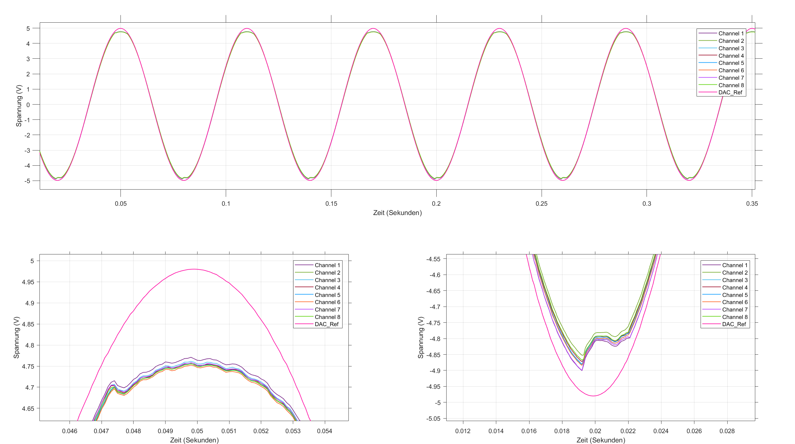
Fig. 240 All DAC output the same sine wave. Due to tolerances in resistor values in the opamp circuit, the amplitudes do not fully match. Additionally, the opamp does not have sufficient headroom and values above \(4.7 V\) and below \(4.75 V\) can not be achieved.#
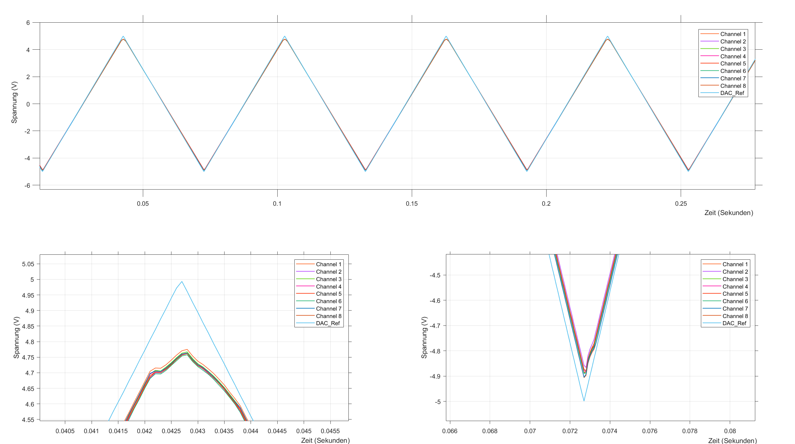
Fig. 241 All DAC output the same triangle wave. Due to tolerances in resistor values in the opamp circuit, the amplitudes do not fully match. Additionally, the opamp does not have sufficient headroom and values above \(4.7 V\) and below \(4.75 V\) can not be achieved.#
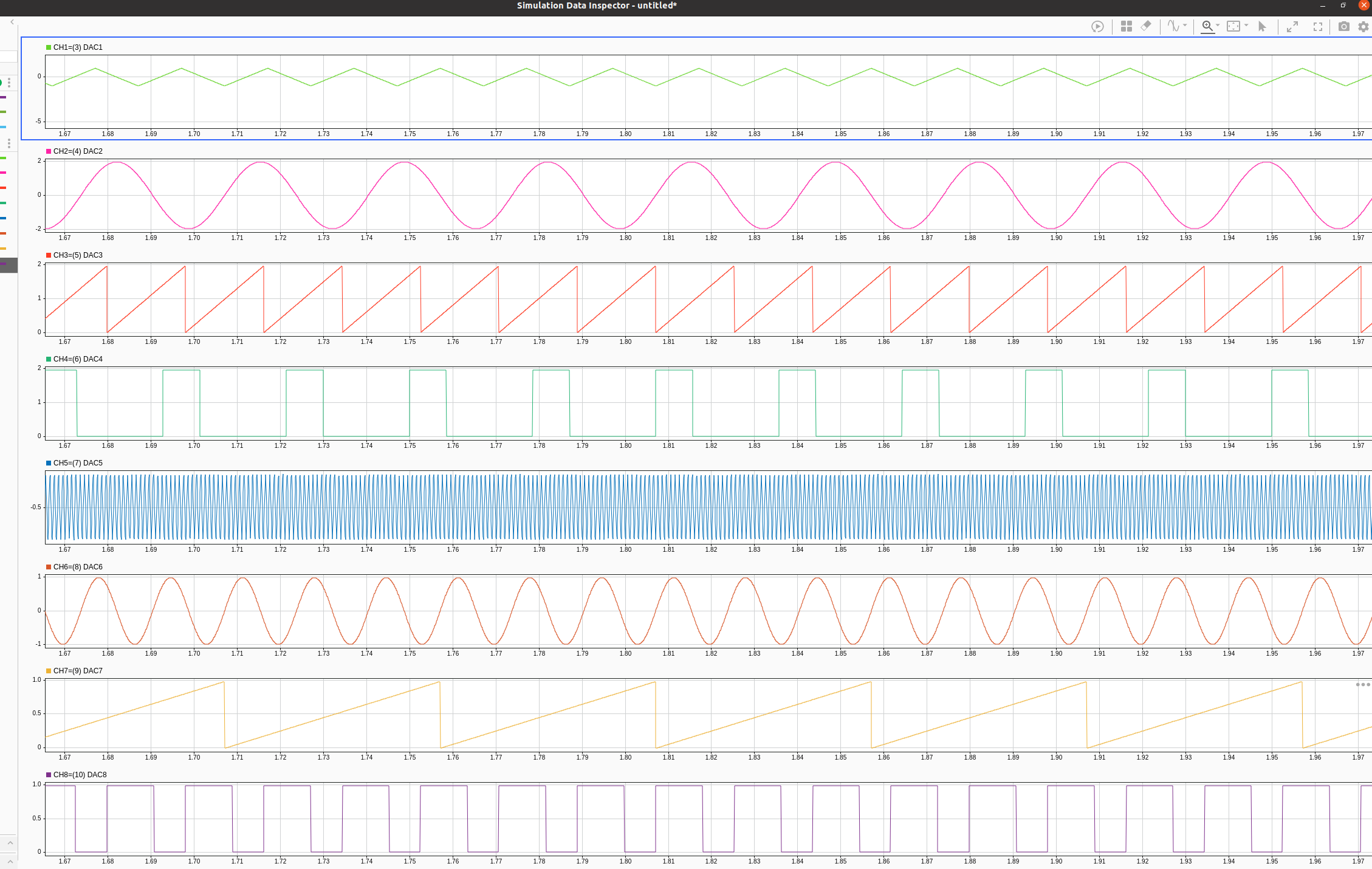
Fig. 242 Different waveforms of Waveform Generator measured in DAC-ADC loopback configuration.#
Warning
The DAC always outputs the last value present in the DAC latch register. The user has to take care of safe DAC output states for the application before stopping control algorithms in the ISR or before flashing the MPSoC during testing.
Pinout#
The pinout of the DAC Ethernet port follows the pinout outlined in Pinout of Analog Connector. See Fig. 231 for the detailed pinout, the ADC number is equal to the DAC number (i.e., ADC1 is DAC1).
Signal name |
pin number (X5-X2) |
|---|---|
CLK_P |
17 |
CLK_N |
19 |
CVN_P |
18 |
CVN_N |
20 |
DAC_IN_P1 |
41 |
DAC_IN_N1 |
43 |
DAC_IN_P2 |
35 |
DAC_IN_N2 |
37 |
DAC_IN_P3 |
29 |
DAC_IN_N3 |
31 |
DAC_IN_P4 |
23 |
DAC_IN_N4 |
25 |
DAC_IN_P5 |
42 |
DAC_IN_N5 |
44 |
DAC_IN_P6 |
36 |
DAC_IN_N6 |
38 |
DAC_IN_P7 |
30 |
DAC_IN_N7 |
32 |
DAC_IN_P8 |
24 |
DAC_IN_N8 |
26 |
References#
Designed by#
Engineer: Michaela Hlatky (TH Nürnberg, ELSYS) in WS 2021/22
Supervision: Tobias Schindler (TH Nürnberg, ELSYS)
Review: Eyke Liegmann (TUM)