Design Rules

Rules are very important for maintaining safety distances. The rules can derive from the requirements regarding voltage and current to the PCB and the requirement, which are given from the PCB manufacturer

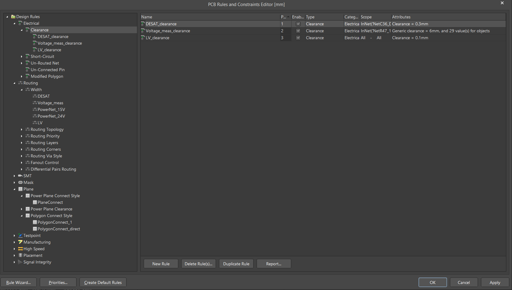
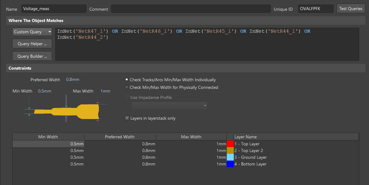
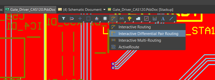
  1. The rule and constraint editor can be opened (only in a PCB document “ .PcbDoc”) Design –> Rules (DR)

../../../_images/160_Design_Rules.png

Fig. 339 Altium - Design Rules Editor.

  1. In this editor many changes and definitions e.g. regarding clearance, routing width, planes, polygons can be made.

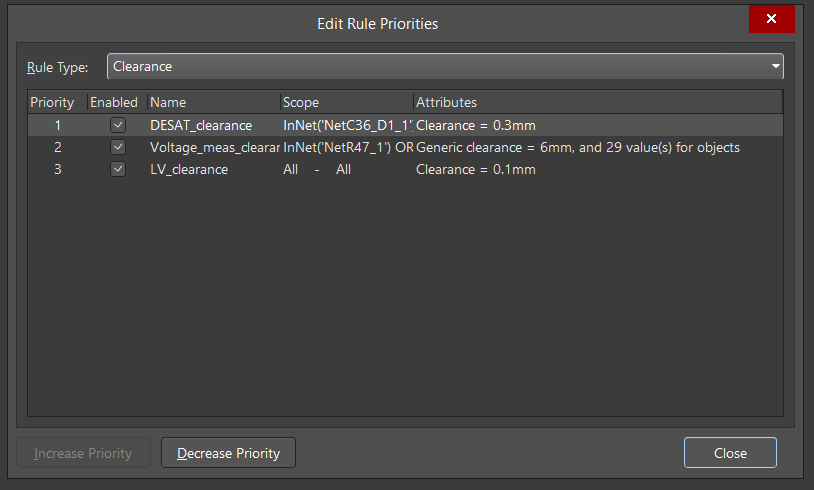
  2. Every rule has a priority, which can be change by choosing the main point like “clearance” (shown in the picture above) + Priorities (on the under edge of this column)

../../../_images/161_Rule_Priorities.png

Fig. 340 Altium - Rules Priorities.

4. In this window you can increase or decrease the priority of the rules regarding the clearance. Every rule needs an exclusive name, which could not be used twice in any rule.

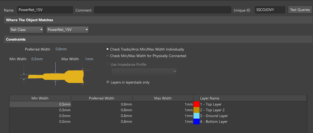
5. The rules can be defined separated for each layer with the help of defining nets (Net Classes are selected by the drop down menu –> PowerNet_15V).

../../../_images/162_Rules_PowerNet.png

Fig. 341 Altium - Defining rules for each layer.

But these nets must be defined in the schematic by making a net label.

../../../_images/163_PowerNet.png

Fig. 342 Altium - Net label.

  1. Furthermore, there is the option to use the “Custom Queries”, where you are able to define dependencies by clauses etc.

../../../_images/164_Rules.png

Fig. 343 Altium - Defining rules by clauses.

These settings must be given by the application and must be individually set before starting with the layout.

Differential signals

Differential signals exist of two signals. Often it is necessary, that these signals have a specific impedance to be robust against malfunctions.

To design suitable parameters for differential signals the open source tool “Saturn PCB Toolkit” is good to use.

Tool Saturn

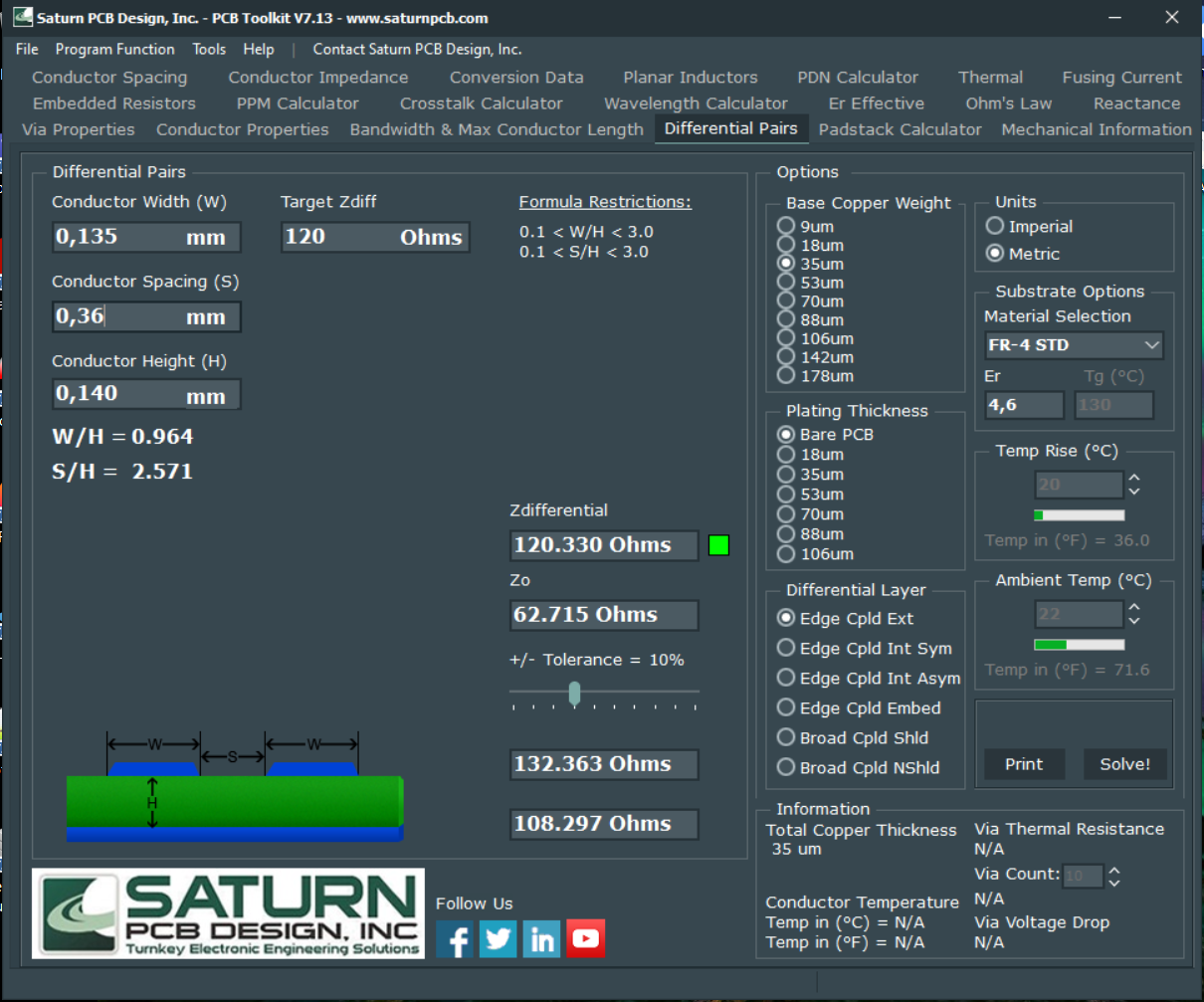
With the help of this tool it is possible to define a target impedance (in that case 120 Ohm) and calculate the necessary conductor width and conductor spacing. The conductor height is given by the height of the layer on which the conductor should be lay outed.

../../../_images/165_Tool_Saturn.png

Fig. 344 Saturn - PCB tool kit.

Altium Rules

If the calculated impedance correspond approximately with the target impedance the values for the conductor width and the conductor spacing can be set in the Altium Rules
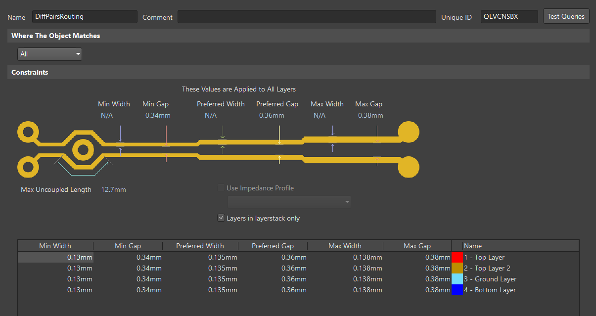
../../../_images/166_Altium_Rules.png

Fig. 345 Altium - Set the calculated values from Saturn in Altium.

Mark Schematic

Before routing these wires it is important to mark these wires with the property “differential pair”.

../../../_images/167_Mark_Schematic.png

Fig. 346 Altium - Marks in schematics.

Route

By routing differential wires use the routing method “Interactive Differential Pair Routing”

../../../_images/168_Route.png

Fig. 347 Altium - Layout differential pairs.