Create a new Altium Project

  1. Open Altium

  2. File –> New –> Project

../../../_images/140_Create_Project.png

Fig. 235 Altium - Create new project.

  1. Give a describing name for the project

  2. Choose a location for saving the project (often it is suitable to save the project in a folder with BitBucket reference)

  3. Click Create

  4. A new project with no content was created

../../../_images/141_New_Project.png

Fig. 236 Altium - New empty project.

  1. Add a new schematic sheet: right mouse click –> Add new to project –> Schematic

  2. Save the new schematic sheet: right mouse click –> save as

../../../_images/142_New_Schematic.png

Fig. 237 Altium - New schematic sheet.

New schematic sheet was added.

9. In general the symbol * marks that this sheet/ project is not saved. This can be done be clicking File –> save or save all

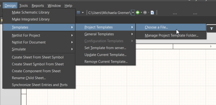
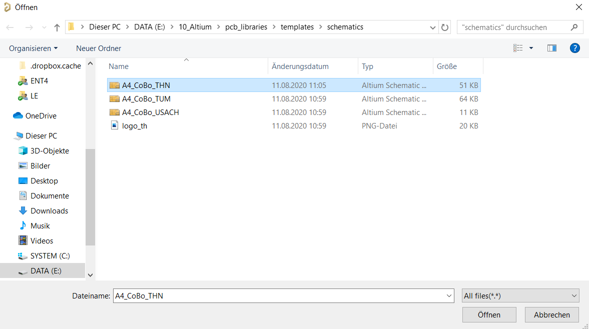
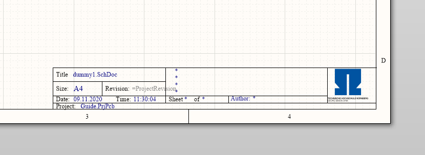
10. If you develop the PCB for the ELSYS institute the template A4_CoBo_THN should be used. It is also part of the BitBucket content and can be found under the following path (for working with BitBucket and Libraries look at the instruction for Altium DB Lib) …pcb_librariestemplatesschematicsA4_CoBo_THN

  1. To use the template in the schematic open the schematic click Design –> Templates –> Project Templates –> Choose a File

../../../_images/143_Template_0.png

Fig. 238 Altium - Choose template.

and select the suitable template

../../../_images/143_Template.png

Fig. 239 Altium - Select template.

  1. Then you get a schematic sheet with this header

../../../_images/144_Template_Sheet.png

Fig. 240 Altium - Templates.

  1. To fill the * marked fields, select the schematic sheet, open the properties (Panels –> Properties)

../../../_images/145_Properties.png

Fig. 241 Altium - Properties.

  1. Change the register from general to parameters

../../../_images/146_Parameters.png

Fig. 242 Altium - Parameters.

  1. Enter the necessary missing parameters

../../../_images/147_Parameters_2.png

Fig. 243 Altium - Parameters.

  1. The result should look like this

../../../_images/148_Templates_2.png

Fig. 244 Altium - Template filled.

  1. The field Project Revision can be neglect or combined with a repository version tool or set manually.

  2. The way for the manual edit process is select Project –> Project Options

  3. Select the register “Parameters”

  4. Add “ProjectRevision” and a value e.g. 0.1

../../../_images/149_Options_PCB.png

Fig. 245 Altium - Options for PCB Project.

  1. Now the schematic workstation is prepared and you are able to place components on the schematic sheet

  2. If components are placed, it is necessary to annotate them by Tools –> Annotate –> Annotate Schematics

../../../_images/150_Annotate_Schematic_1.png

Fig. 246 Altium - Annotate schematic.

  1. Update Changes List

../../../_images/150_Annotate_Schematic_2.png

Fig. 247 Altium - Update Changes List.

  1. OK

../../../_images/150_Annotate_Schematic_3.png

Fig. 248 Altium - OK.

  1. Accept Changes (Create ECO)

../../../_images/150_Annotate_Schematic_4.png

Fig. 249 Altium - Accept Changes.

  1. Validate Changes –> Execute Changes –> Close

../../../_images/150_Annotate_Schematic_5.png

Fig. 250 Altium - Validate/ Execute/ Close.

27. Every component should have a designator. Most important thing is to be consistent within one project. See Wikipedia for an example list.

../../../_images/150_Annotate_Schematic_6.png

Fig. 251 Altium - Designator D1.

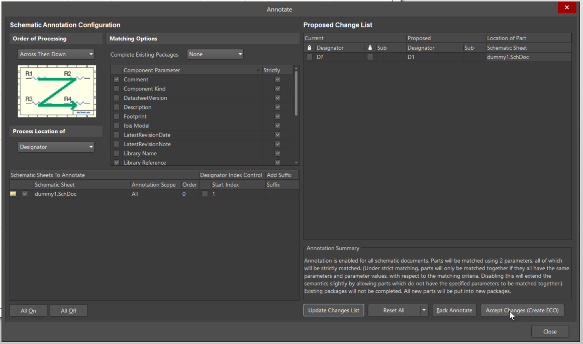
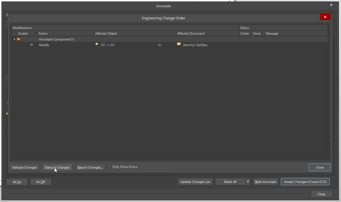
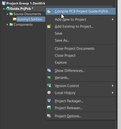
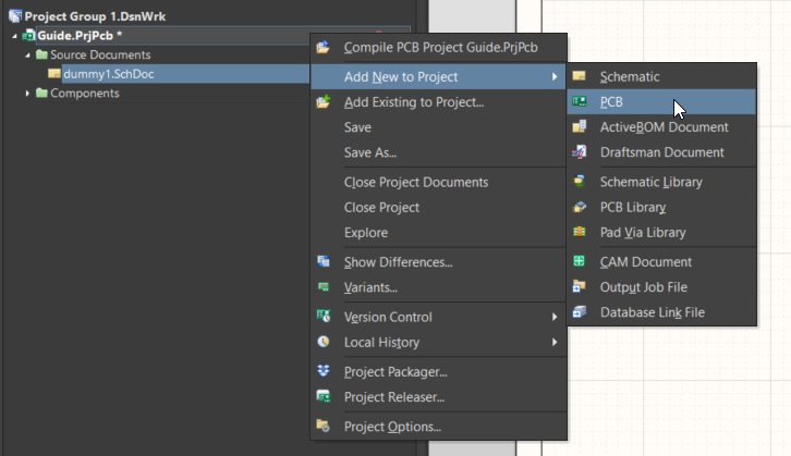
  1. If you placed some components on the schematic sheet(s) and annotated them compile the project right mouse click on the project –> Compile PCB Project Guide.PrjPcb

../../../_images/150_Compile_Project.png

Fig. 252 Altium - Compile Project.

If errors exist –> debug problems

If no errors –> create PCB

  1. Create PCB

Right mouse click –> Add new to project –> PCB

../../../_images/150_Add_PCB.png

Fig. 253 Altium - Add PCB to project.

  1. Save PCB

Right mouse click –> Save as

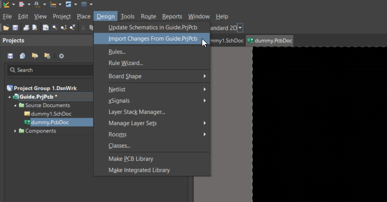
  1. Import Components from the schematic to the PCB Design –> Import Changes from Guide.PrjPcb (short cut: di)

../../../_images/150_PCB.png

Fig. 254 Altium - Import components from schematic.

Be careful not to use Update Changes from Guide.PrjPcb. In this case you update the schematic with no content of the PCB. 
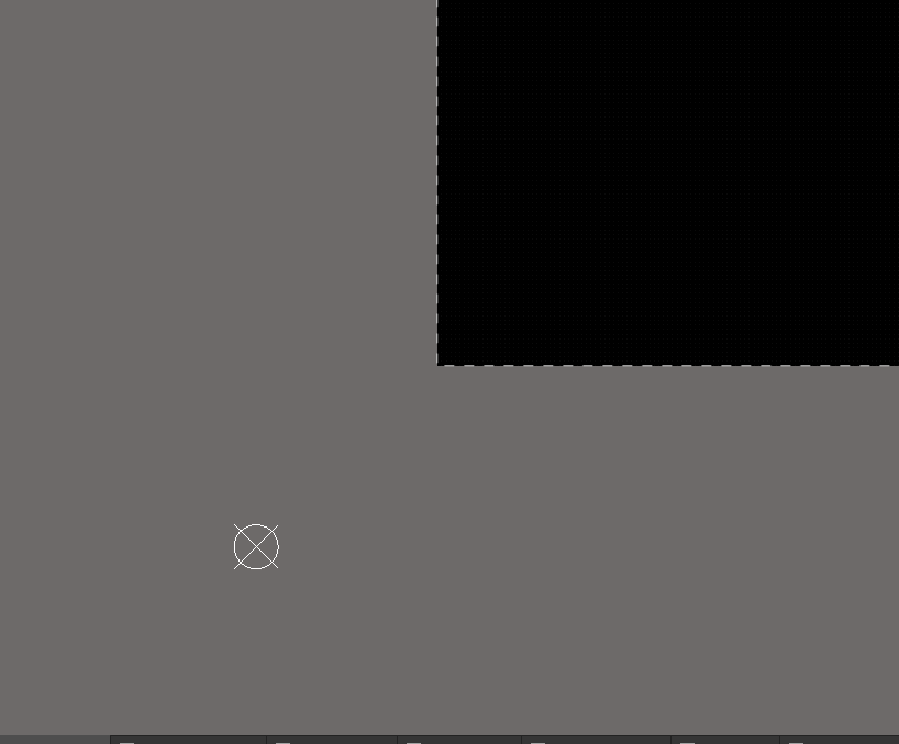
All components included in the schematic sheets are placed on the right edge of the PCB.

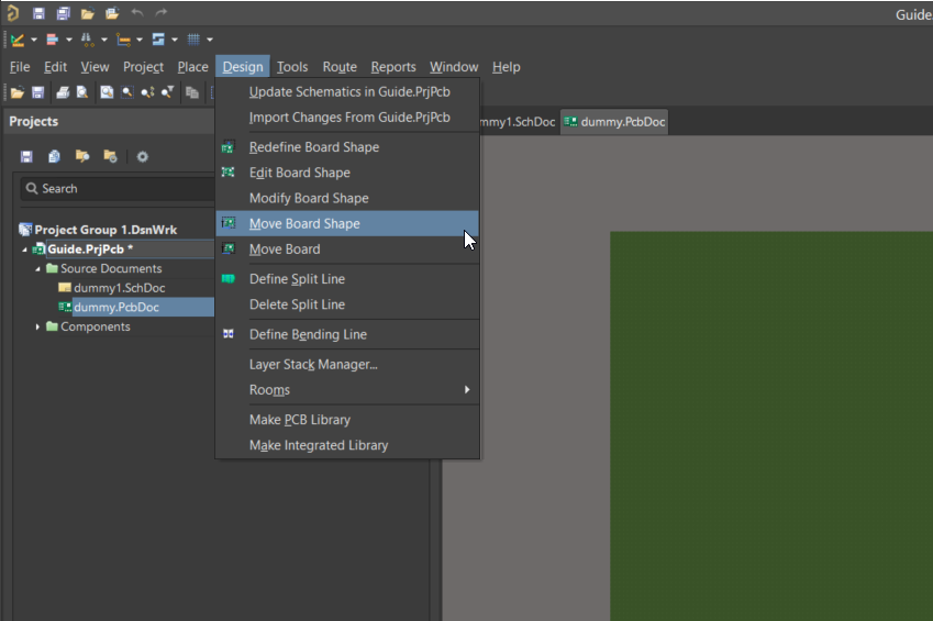
By pressing the numbers 1, 2 and 3 you can select between the following views

1 = Board planning mode –> define the shape of the PCB

2 = 2D view –> routing view

3 = 3D view

Often it is helpful to define the null- point on the left corner because then the x and y dimension is without any offset

To do this:

  1. Open the created PCB

../../../_images/151_Change_Board_Shape.png

Fig. 255 Altium - Open PCB.

  1. Go to board planing mode by clicking 1

  2. Design –> move board shape –> move it to the x

../../../_images/152_Change_Board_Shape_0.png

Fig. 256 Altium - Select move board shape.

../../../_images/152_Change_Board_Shape.png

Fig. 257 Altium - Move the board in the corner.

4. Go back to the layout view (2) and start with the configuration of the layer stack –> have a look at the chapter PCB Layer Stack Manager