Digital Resolver Rev01#
Source#
Interface and Functionality#
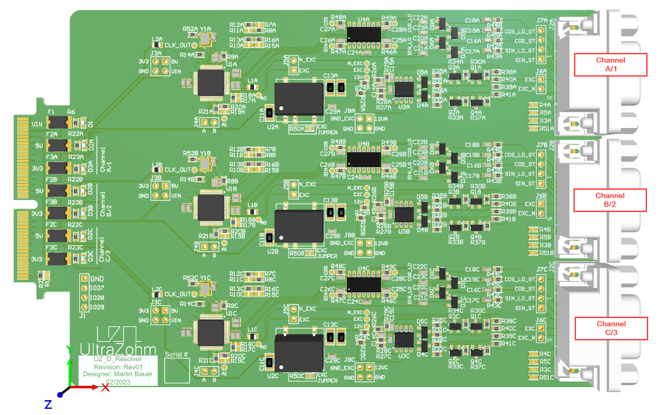
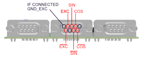
The UltraZohm digital resolver adapter board features three channels of resolver interfaces, including excitation signal generation and serial interfaces. Each channel is based on the AD2S1210 integrated-circuit. The board features separated grounds for each channel of the excitation circuit (GND_EXC), which can be connected to the common logic ground via a resistor. Each resolver channel can be configured with several pull-up and pull-down resistors. Default configuration sets:
RES0andRES1toHIGH- max resolution of 16 bitRDtoHIGH- output buffer disabled asSOEto LOW - Serial Interface is selected (this adapter card is only to be operated in serial configuration)Excitation Ground
GND_EXC[1..3]andGNDconnected (RemoveR50[A..C]to disconnect the grounds)Excitation Ground
GND_EXC[1..3]connecting resistors to DSUB ConnectorsJ2[A..C]NOT connected (Place 0 Ohm atR3,R4,R5andR51each[A..C]to connect grounds)N_SAMPLEto HIGH (also see known issues section for this)
Note
The clock speed of the Clock in Rev01 is 8.192 MHz, which is relevant to the Specifications of the AD2S1210 IC
Note
As the resolver only operates with the 16 bit resolution in the board’s default configuration, the measurable rotational speed is limited to 125 rounds per second (rps) (equals \(7500\frac{1}{min}\)) with a clock speed of 8.192 MHz. For higher speeds the resolution has to be lowered. This affects RES0 and RES1 resistor configuration as well as IP core driver configuration.
With the Signals A0 and A1 the resolver`s operation mode can be configured. This is done through the IP core driver:
A0to LOW andA1to LOW = Normal mode - position outputA0to LOW andA1to HIGH = Normal mode - velocity outputA0to HIGH andA1to LOW = Reserved (not used)A0to HIGH andA1to HIGH = Configuration Mode
In position and velocity mode the corresponding data can be obtained directly by toggling the clock line without sending the register addresses first. Further access to the devices registers and configurations is possible in the configuration mode. In this mode, changing the excitation frequency or reading back position and velocity data is possible. This is equivalent to Digital Encoder 1v00.
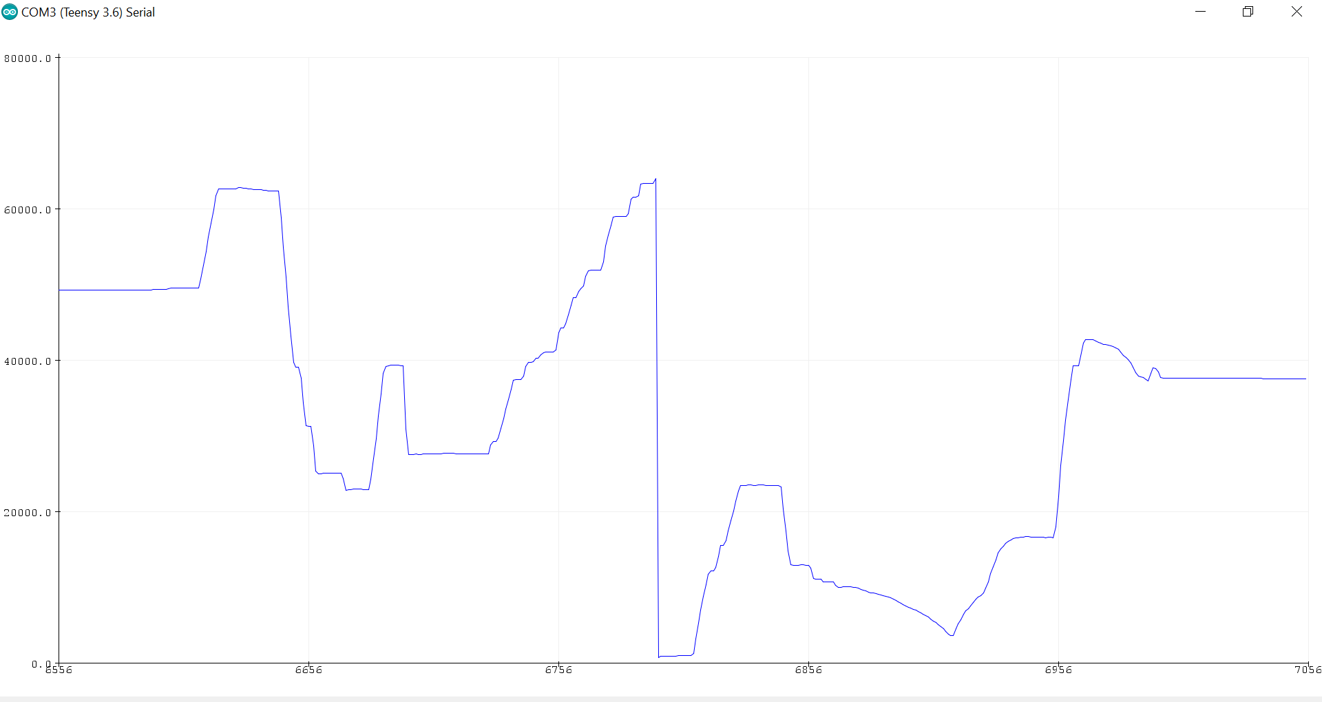
Fig. 277 Position Data from Resolver#
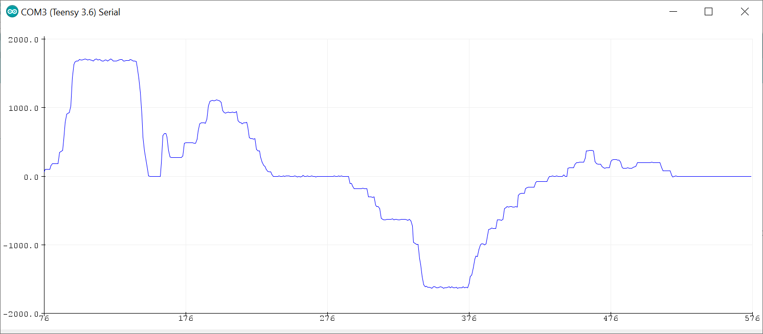
Fig. 278 Velocity Data from Resolver#
When communicating with the controller, attention has to be paid on the SPI mode. The correct one is MODE1 with clock polarity idle low and clock phase one meaning falling edge.
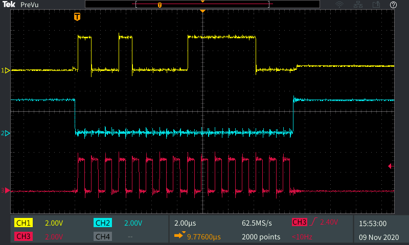
Fig. 279 Data Transmission in normal mode (position or velocity), yellow: MISO, blue: FSYNC, red: CLK#
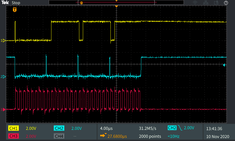
Fig. 280 Data Transmission in config mode, yellow: MISO, blue: FSYNC, red: CLK#
Before first use#
Determine correct placement options for correct function (Default is 16-bit resolution) and one common GND for all channels
Program CPLD with proper firmware, uz_d_resolver CPLD program. See Programming the CPLD for details.
Warning
There are two different CPLD programs in the cpld_lattice repository for uz_d_resolver. One for usage of the adapter board in slots D1 to D4 (sub-folder: digital_D1_to_D4). And a special one for usage in slot D5 (sub-folder: digital_D5). Due to the limited number of pins at D5 there are only two resolver channels available (Ch A/1 and Ch B/2).
Known issues#
Warning
N_SAMPLE is pulled to HIGH using 5V on Rev01. It should be 3V3 to ensure safe operation of the AD2S1210 IC. This has been fixed for Rev02. Before first use of Rev01 boards, carefully check, if resistors R14[A..C] are NOT placed.
Compatibility#
This Board is compatible with slots D1-D5. In Slot D5 only CH A/1 and CH B/2 are available. Also, there is a special CPLD program needed for D5, D1 to D4 share a common CPLD program
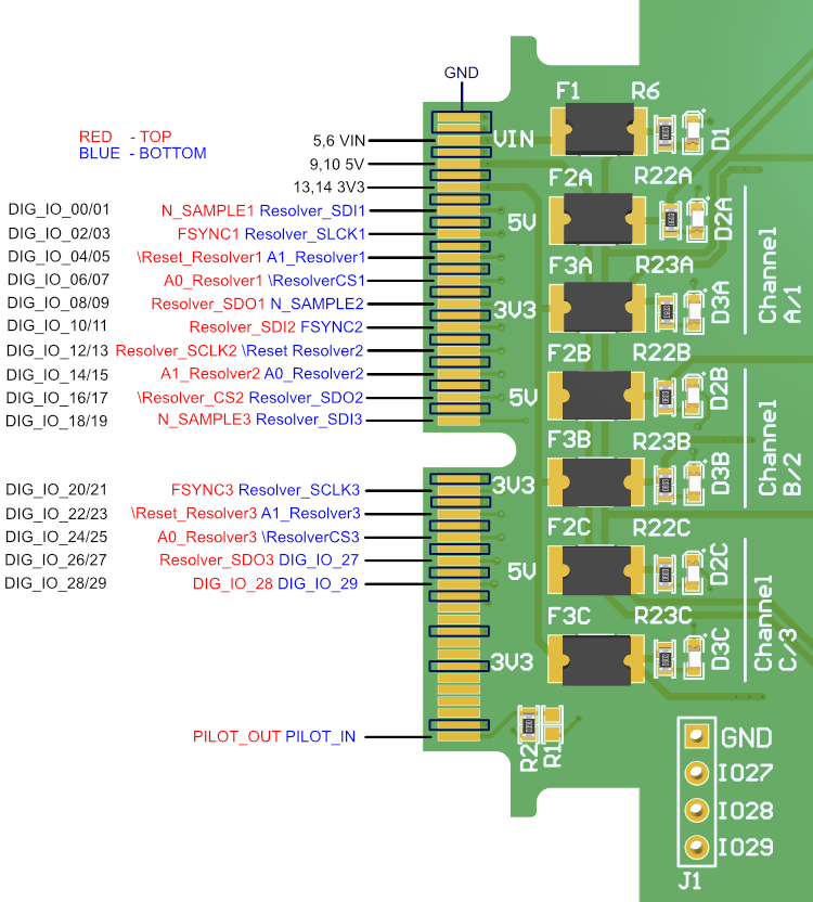
Pinout#
Pin Number |
Signal |
|---|---|
1 |
IF CONNECTED: GND_EXC |
2 |
COS |
3 |
SIN |
4 |
EXC |
5 |
IF CONNECTED: GND_EXC |
6 |
-COS |
7 |
-SIN |
8 |
IF CONNECTED: GND_EXC |
9 |
-EXC |
Implementation with Resolver Interface IP Core#
The following describes the connecting of the adapter board with the resolver interface IP cores.
Two cases have to be distinguished here:
3 channels in slot D1 to D4,2 channels in slot D5
In general one has to add the Resolver Interface IP core e.g. to the user hierarchy in the block design as many times as channels are needed.
The port names of the IP core and at the adapterboard slightly differ. Therefore it is useful to create ports at the user hierarchy with the adapter boards’ signal names in order to avoid confusion.
E.g. the picture below shows the IP core and respective ports for channel A/1. Pay attention to the signals SDI and SDO. Depending on the perspective, serial data in and out can change.
In this example it is seen from the FPGA perspective, therefore, SPI_MOSI is labeled to SDO_1.
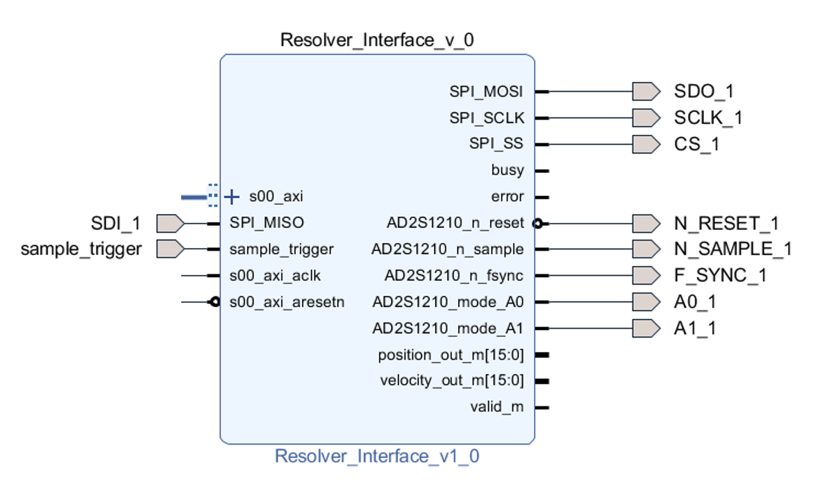
Outside the user hierarchy it then depends on the physical adapter board slot that you are using, what signal has to be connected to which pin.
Again, pay attention to SDI and SDO signals. Now we connect the signals to the adapter card pins. Here, our SDO signal from the block design
has to be connected to the pin number that provides the SDI signal of the adapter board and vice versa.
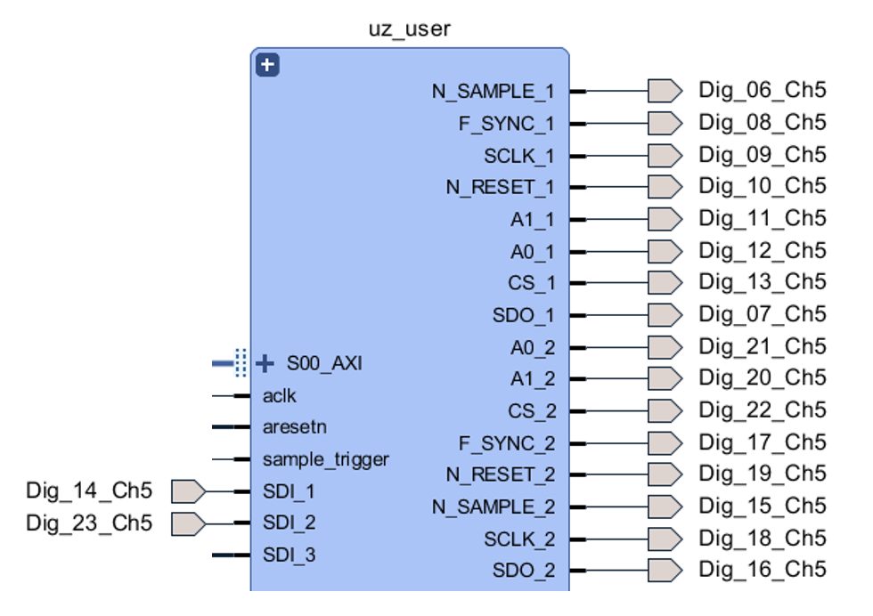
2 Channels in Slot D5 (Ch A/1 and Ch B/2)#
The constraint file for slot D5 gives by default access to every single pin using the naming convention Dig_xx_Ch5, where xx is the I/O number [00…29].
Simply create input and output ports as shown below and connect them.
3 Channels in Slots D1 to D4#
Below you’ll find an example on how to use the adapter board in slot D4. By default the constraint file for D4 is written in a vectorized (packed) manner that is not proper for accessing single pins.
But there are also constraint files provided that allow access to the single pins. As shown below find the files in the sources section in Vivado. Right click on Digital_D4_packed.xdc and Disable File.
Then right click on Digital_AdapterBoard_D4.xdc and Enable File.
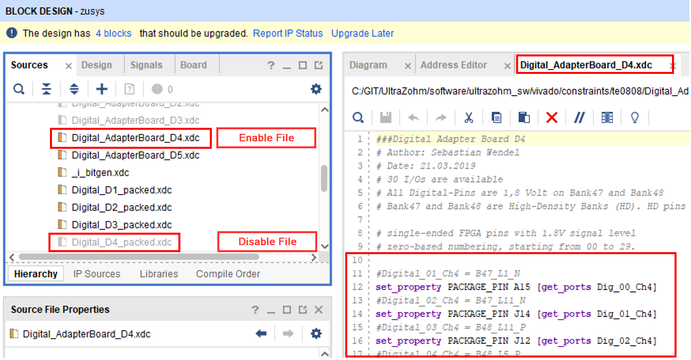
Now we can access D4 pins with the same naming convention as above and create and connect respective ports as shown in the picture below.
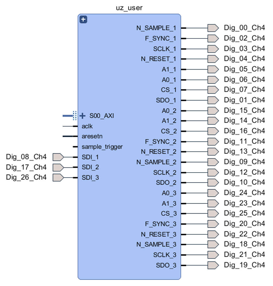
Finally do not forget to connect IP core clocks (100 MHz) and AXI interfaces, as well as a proper sampling_trigger signal (e.g. trigger_conversion signal that also triggers the ADC’s).
Build the bitstream and see the respective IP core driver docs for the software part.
References#
Designed by#
Martin Bauer (THN), Eyke Aufderheide (TUM) in 02/2022 based on design by Thomas Effenberger (TUM)