Interfaces#

The carrier board has the following interfaces.
Name |
Function |
|---|---|
J1 |
SoM |
J2 |
SoM |
J3 |
SoM |
J4 |
SoM |
X1 |
CPLD JTAG |
X2 |
CPLD Jumper |
X3 |
Interface to CPLD of X6E |
X4 |
Ethernet |
X5A |
Analog adapter card A1 |
X5B |
Analog adapter card A2 |
X5C |
Analog adapter card A3 |
X6A |
Digital adapter card D1 |
X6B |
Digital adapter card D2 |
X6C |
Digital adapter card D3 |
X6D |
Digital adapter card D4 |
X6E |
Digital adapter card D5 with fewer FPGA pins |
X7A |
CAN1 |
X7A |
CAN2 |
X8 |
MPSoC JTAG |
X9 |
(PS JTAG - not assembled) |
X10 |
PS SPI - UART - I2C |
X11 |
(USB - not assembled) |
X12 |
SPI |
X13 |
PS GPIO |
X14 |
Power in (24 V) |
X15 |
Power out (24 V) |
X16 |
SD-Card |
X1: CPLD-JTAG#
JTAG interface to all CPLDs for D1 to D5. You can use a Trenz TE0590 programmer ( see Programming the CPLD).
Pin on X1 |
Signal |
Function |
Direction |
|---|---|---|---|
1 |
GND |
Ground |
|
2 |
GND |
Ground |
|
3 |
A |
not connected |
|
4 |
C |
CPLD TCK (clock line) |
input |
5 |
3.3 V |
connected with 3V3_PER |
output |
6 |
VIO |
connected with 3V3_PER |
output |
7 |
B |
not connected |
|
8 |
D |
CPLD TDO (serial data out) |
output |
9 |
E |
not connected |
|
10 |
F |
CPLD TDI (serial data in) |
input |
11 |
G |
not connected |
|
12 |
H |
CPLD TMS (mode select) |
input |
X2: CPLD-Jumper#
Pin header connector to set jumper for individual programmaing of the CPLDs. If you would like to program all five CPLDs at once, you have to link them together as a daisy chain: set jumper to 1-2, 3-4, 5-6, 7-8, 9-10, 11-12. (see Programming the CPLD)
Pin on X2 |
Signal |
Function |
Direction |
|---|---|---|---|
1 |
CPLD TDI |
TDI connection from programmer |
output |
2 |
CPLD_TDI1 |
TDI from CPLD 1 |
input |
3 |
CPLD_TDO1 |
TDO from CPLD 1 |
output |
4 |
CPLD_TDI2 |
TDI from CPLD 2 |
input |
5 |
CPLD_TDO2 |
TDO from CPLD 2 |
output |
6 |
CPLD_TDI3 |
TDI from CPLD 3 |
input |
7 |
CPLD_TDO3 |
TDO from CPLD 3 |
output |
8 |
CPLD_TDI4 |
TDI from CPLD 4 |
input |
9 |
CPLD_TDO4 |
TDO from CPLD 4 |
output |
10 |
CPLD_TDI5 |
TDI from CPLD 5 |
input |
11 |
CPLD_TDO5 |
TDO from CPLD 5 |
output |
12 |
CPLD TDO |
TDO connection to programmer |
input |
X3: CPLD-X6E (D5)#
Not all 30 digital signals of X6E is fully connected to the FPGA. X3 is routed to the primary side (1.8 V) of the CPLD. The factory CPLD software routes these signals of X3 to the X6E pins DIG_01 to DIG06 and DIG_25 to DIG_30. The direction of the signals can be determined with your user CPLD software code. The factory default is input.
Pin on X3 |
Signal |
Function |
Direction |
Specification |
|---|---|---|---|---|
1 + 10 + 11 + 20 |
3V3_PER |
power supply |
output |
3.3 V / 150 mA |
2 + 9 + 12 + 19 |
GND |
Ground |
||
3 |
DIG_05_Ch5 |
digital I/O |
input |
1.8 V / 8 mA |
4 |
DIG_03_Ch5 |
digital I/O |
input |
1.8 V / 8 mA |
5 |
DIG_01_Ch5 |
digital I/O |
input |
1.8 V / 8 mA |
6 |
DIG_29_Ch5 |
digital I/O |
input |
1.8 V / 8 mA |
7 |
DIG_27_Ch5 |
digital I/O |
input |
1.8 V / 8 mA |
8 |
DIG_25_Ch5 |
digital I/O |
input |
1.8 V / 8 mA |
13 |
DIG_06_Ch5 |
digital I/O |
input |
1.8 V / 8 mA |
14 |
DIG_04_Ch5 |
digital I/O |
input |
1.8 V / 8 mA |
15 |
DIG_02_Ch5 |
digital I/O |
input |
1.8 V / 8 mA |
16 |
DIG_30_Ch5 |
digital I/O |
input |
1.8 V / 8 mA |
17 |
DIG_28_Ch5 |
digital I/O |
input |
1.8 V / 8 mA |
18 |
DIG_26_Ch5 |
digital I/O |
input |
1.8 V / 8 mA |
X4: Ethernet#
This RJ45 connector is used for Ethernet communication. You can use standard LAN cables.
X5: Analog adapter#
The board connector X5 is used to connect analog adapter boards to the carrier board. X5A to X5C features each 10 differential signals, which are routed (impedance controlled) directly to the FPGA at a voltage level of 1.8 V with LVDS standard. The drive strength of the FPGA pins is configurable (4, 8, 12 or 16 mA) by software in Vivado. For more information see in Xilinx documentation. Additionally, there is shared SPI and I2C available on X5.
Pin on X5 |
Name |
Specification |
|---|---|---|
5 + 6 |
VIN |
24 V / 400 mA |
9 + 10 |
5V_PER |
5 V / 500 mA |
13 + 14 |
3V3_PER |
3.3 V / 300 mA |
Name |
Interface |
Pin on X5 |
Bank |
Type |
Specification |
|---|---|---|---|---|---|
A1 |
X5A |
1-9 |
Bank 64 |
High Performance (HP) |
1.8 V / 12 mA LVDS |
A1 |
X5A |
10 |
Bank 65 |
High Performance (HP) |
1.8 V / 12 mA LVDS |
A2 |
X5B |
1-8 |
Bank 64 |
High Performance (HP) |
1.8 V / 12 mA LVDS |
A2 |
X5B |
9 |
Bank 65 |
High Performance (HP) |
1.8 V / 12 mA LVDS |
A2 |
X5B |
10 |
Bank 64 |
High Performance (HP) |
1.8 V / 12 mA LVDS |
A3 |
X5C |
1 |
Bank 65 |
High Performance (HP) |
1.8 V / 12 mA LVDS |
A3 |
X5C |
2-3 |
Bank 65 |
High Performance (HP) |
1.8 V / 12 mA LVDS |
A3 |
X5C |
4 |
Bank 65 |
High Performance (HP) |
1.8 V / 12 mA LVDS |
A3 |
X5C |
5 |
Bank 64 |
High Performance (HP) |
1.8 V / 12 mA LVDS |
A3 |
X5C |
6 |
Bank 65 |
High Performance (HP) |
1.8 V / 12 mA LVDS |
A3 |
X5C |
7-8 |
Bank 64 |
High Performance (HP) |
1.8 V / 12 mA LVDS |
A3 |
X5C |
9-10 |
Bank 65 |
High Performance (HP) |
1.8 V / 12 mA LVDS |
Pin on X5 |
Signal |
Function |
Direction |
Specification |
|---|---|---|---|---|
47 |
SPI_shared_MOSI |
master out slave in |
output |
3.3 V / 12 mA |
48 |
SPI_shared_CLK |
clock |
output |
3.3 V / 12 mA |
53 |
SPI_shared_CS |
chip select |
output |
3.3 V / 12 mA |
Pin on X5 |
Signal |
Function |
Direction |
Specification |
|---|---|---|---|---|
54 |
CS_fastADC |
chip select fast ADC |
output |
3.3 V / 12 mA |
Pin on X5 |
Signal |
Function |
Direction |
Specification |
|---|---|---|---|---|
55 |
PL_ANL_GPIO_01 |
general purpose I/O from FPGA |
input/output |
3.3 V / 10 mA |
56 |
PS_ANL_GPIO_01 |
general purpose I/O from processing system |
input/output |
3.3 V / 10 mA |
59 |
PS_ANL_GPIO_02 |
general purpose I/O from processing system |
input/output |
3.3 V / 10 mA |
The reserved pins of the X5 connector are currently attached with test points on the carrier board. They are reserved for future purposes.
Pin on X5 |
Signal |
Function |
Direction |
Specification |
|---|---|---|---|---|
60 |
ANL_Res_01 |
reserved pin |
||
61 |
ANL_Res_02 |
reserved pin |
||
62 |
ANL_Res_03 |
reserved pin |
||
65 |
ANL_Res_04 |
reserved pin |
||
66 |
ANL_Res_05 |
reserved pin |
||
67 |
ANL_Res_06 |
reserved pin |
||
68 |
ANL_Res_07 |
reserved pin |
||
71 |
ANL_Res_08 |
reserved pin |
||
72 |
ANL_Res_09 |
reserved pin |
||
73 |
ANL_Res_10 |
reserved pin |
||
74 |
ANL_Res_11 |
reserved pin |
||
77 |
ANL_Res_12 |
reserved pin |
The collective fault signal is an error signal that can be provided from each adapter card and will be evaluated on the carrier board.
Pin on X5 |
Signal |
Function |
Direction |
Specification |
|---|---|---|---|---|
78 |
Collective_FLT |
collective fault |
input |
3.3 V / 20 mA |
Pin on X5 |
Signal |
Function |
Direction |
Specification |
|---|---|---|---|---|
79 |
PILOT_OUT |
pilot line out |
output |
3.3 V / hi-Z |
80 |
PILOT_IN |
pilot line in |
input |
3.3 V / hi-Z |
X6: Digital adapter#
The board connector X6 is used to connect digital adapter boards to the carrier board. X6 has 30 I/Os (DIG_IO_01 to DIG_IO_30) with a voltage level of 3.3 V which are routed to a CPLD for each digital interface. The I/O signals from X6A, X6B, X6C, X6D are routed via the CPLD to the SoM (J1 to J4). X6E features 30 I/Os of which 12 (DIG_01 to DIG_06 and DIG_25 to DIG_30) are routed from the CPLD to X3 and the other 18 I/Os are routed to the FPGA.
Pin X6 |
Name |
Specification |
|---|---|---|
5 + 6 |
VIN |
24 V / 400 mA |
9 + 10 |
5V_PER |
5.0 V / 500 mA |
13 + 14 |
3V3_PER |
3.3 V / 300 mA |
Name |
Interface |
X6-PIN |
Bank |
Type |
|---|---|---|---|---|
D1 |
X6A |
1-30 |
Bank 65 |
High Performance (HP) |
D2 |
X6B |
1-14 |
Bank 66 |
High Performance (HP) |
D2 |
X6B |
25-30 |
Bank 66 |
High Performance (HP) |
D2 |
X6B |
15-24 |
Bank 65 |
High Performance (HP) |
D3 |
X6C |
1-30 |
Bank 66 |
High Performance (HP) |
D4 |
X6D |
1-2 |
Bank 47 |
High Density (HD) |
D4 |
X6D |
3-24 |
Bank 48 |
High Density (HD) |
D4 |
X6D |
25-30 |
Bank 47 |
High Density (HD) |
D5 |
X6E |
7-8 |
Bank 66 |
High Performance (HP) |
D5 |
X6E |
9-24 |
Bank 47 |
High Density (HD) |
Pin on X6 |
Signal |
Function |
Direction |
Specification |
|---|---|---|---|---|
77 |
PS_DIG_GPIO_01 |
general purpose I/O from processing system |
input/output |
3.3 V / 10 mA |
78 |
PS_DIG_GPIO_02 |
general purpose I/O from processing system |
input/output |
3.3 V / 10 mA |
Pin on X6 |
Signal |
Function |
Direction |
Specification |
|---|---|---|---|---|
83 |
CPLD_DigIn_01 |
general purpose input from CPLD |
input |
3.3 V / 8 mA |
84 |
CPLD_DigOut_01 |
general purpose output from CPLD |
output |
3.3 V / 8 mA |
85 |
CPLD_DigIn_02 |
general purpose input from CPLD |
input |
3.3 V / 8 mA |
86 |
CPLD_DigOut_02 |
general purpose output from CPLD |
output |
3.3 V / 8 mA |
Pin on X6 |
Signal |
Function |
Direction |
Specification |
|---|---|---|---|---|
89 |
I2C0_SCL |
I2C bus from processing system |
bi-directional |
3.3 V / 10 mA |
90 |
I2C0_SDA |
I2C bus from processing system |
bi-directional |
3.3 V / 10 mA |
The reserved pins of the X6 connector are currently attached with test points on the carrier board. They are reserved for future purposes.
Pin on X6 |
Signal |
Function |
Direction |
Specification |
|---|---|---|---|---|
79 |
DIG_Res_01 |
reserved pin |
||
80 |
DIG_Res_02 |
reserved pin |
||
91 |
DIG_Res_03 |
reserved pin |
||
92 |
DIG_Res_04 |
reserved pin |
||
93 |
DIG_Res_05 |
reserved pin |
||
94 |
DIG_Res_06 |
reserved pin |
||
95 |
DIG_Res_07 |
reserved pin |
The collective fault signal is an error signal that can be provided from each adapter card and will be evaluated on the carrier board.
Pin on X6 |
Signal |
Function |
Direction |
Specification |
|---|---|---|---|---|
96 |
Collective_FLT |
collective fault |
input |
3.3 V / 20 mA |
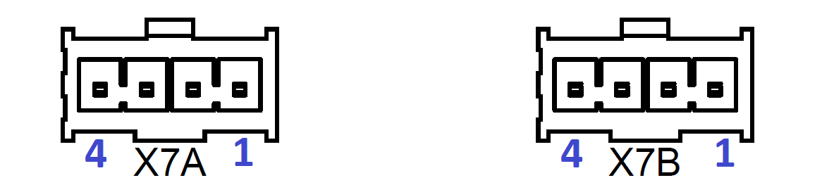
X7: Isolated CAN#
The following applies to X7A and X7B:
This connectors are used for CAN. X7A is labeled with CAN1 and X7B with CAN2 on the PCB.
The CAN interface is operated by the processor.
The connector X7A uses
CAN_0and X7BCAN_1in the processor.The pins are isolated and have a voltage level of 5V.
The CAN termination resistors (120 Ohm) are assembled by default (R76A - R77A, R76B - R77B) and can be found with the assembly drawing
(LINK).
Pin on X7 |
Signal |
Function |
Direction |
Specification |
|---|---|---|---|---|
1 |
5V_isoCAN |
isolated power supply |
output |
5 V / 100 mA |
2 |
CAN_H |
can high |
bi-directional |
|
3 |
CAN_L |
can low |
bi-directional |
|
4 |
GND_isoCAN |
isolated ground |
X8: MPSoC-JTAG#
JTAG interface for the MPSoC.
Pin on X8 |
Signal |
Function |
Direction |
Specification |
|---|---|---|---|---|
1 |
GND |
Ground |
||
2 |
GND |
Ground |
||
3 |
PS_UART0_TX |
UART transmit |
output |
xx V / xx mA |
4 |
TCK |
JTAG clock |
input |
xx V / xx mA |
5 |
3V3_PER |
power supply of programmer (not assembled by default) |
output |
3.3V / 100 mA |
6 |
PS_1V8 |
power supply of processing system |
output |
1.8 V / xx mA |
7 |
PS_UART0_RX |
UART receive |
input |
xx V / xx mA |
8 |
TDO |
JTAG data out |
output |
xx V / xx mA |
9 |
not connected |
|||
10 |
TDI |
JTAG data in |
input |
xx V / xx mA |
11 |
MR |
xx V / xx mA |
||
12 |
TMS |
JTAG mode select |
input |
xx V / xx mA |
X9: PS-JTAG#
JTAG interface to JTAG - not assembled!
X10: Serial bus#
Interface to serial buses (UART1, SPI0, I2C1) of the processing system (PS) for external devices. The interface is not isolated.
Pin on X10 |
Signal |
Function |
Direction |
Specification |
|---|---|---|---|---|
1 + 7 |
3V3_PER |
power supply |
output |
3.3 V / 150 mA |
2 + 8 |
GND |
Ground |
||
3 |
EXT_SPI0_MOSI |
SPI master out slave in |
output |
3.3 V / 10 mA |
4 |
EXT_SPI0_SCLK |
SPI clock |
output |
3.3 V / 10 mA |
5 |
EXT_UART1_RX |
UART receive |
input |
3.3 V / 10 mA |
6 |
EXT_I2C1_SCL |
I2C serial clock |
bi-directional |
3.3 V / 10 mA |
9 |
EXT_SPI0_MISO |
SPI master in slave out |
input |
3.3 V / 10 mA |
10 |
EXT_SPI0_CS |
SPI chip select |
output |
3.3 V / 10 mA |
11 |
EXT_UART1_TX |
UART transmit |
output |
3.3 V / 10 mA |
12 |
EXT_I2C1_SDA |
I2C serial data |
bi-directional |
3.3 V / 10 mA |
X11: USB#
Interface to USB of PS - not assembled!
X12: Isolated SPI1#
Isolated SPI1 of processing system (PS).
Pin on X12 |
Signal |
Function |
Direction |
Specification |
|---|---|---|---|---|
1 |
3V3_isoSPO |
isolated power supply |
output |
3.3 V / 100 mA |
2 |
isoSPI_MOSI_3V3 |
isolated SPI master out slave in |
output |
3.3 V / 20 mA |
3 |
isoSPI_MISO_3V3 |
isolated SPI master in slave out |
input |
3.3 V / 20 mA |
4 |
GND_isoSPI |
isolated SPI ground |
||
5 |
isoSPI_SCLK_3V3 |
isolated SPI clock |
output |
3.3 V / 20 mA |
6 |
isoSPI_CS_3V3 |
isolated SPI chip select |
output |
3.3 V / 20 mA |
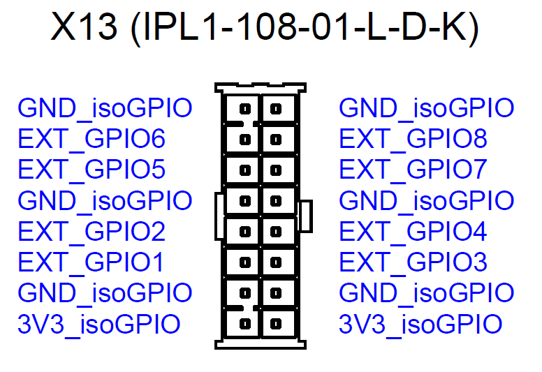
X13: Isolated PS GPIO Pins#
This connector is used for the front panel LEDs. However, it is not limited to this.
This connector offers eight GPIOs from the processor (MIO Pins).
The pins are isolated and have a voltage level of 3.3 V.
The direction is given by the isolator chips U24 and U26.
Pin connection:
Pin on X13 |
Signal |
non-isolated Signal |
Carrier Board LED |
Front Panel |
Function |
Direction |
Specification |
|---|---|---|---|---|---|---|---|
1 + 9 |
3V3_isoGPIO |
n.c. |
isolated power supply |
output |
3.3 V / 100 mA |
||
2 |
GND_isoGPIO |
Ready_GND |
Ground |
||||
3 |
EXT_GPIO1 |
PS_GPIO1 |
LED1 |
Ready_VCC |
output |
3.3 V / 20 mA |
|
4 |
EXT_GPIO2 |
PS_GPIO2 |
LED2 |
Running_VCC |
output |
3.3 V / 20 mA |
|
5 |
GND_isoGPIO |
Running_GND |
Ground |
||||
6 |
EXT_GPIO5 |
PS_GPIO5 |
n.c. |
input |
3.3 V / 20 mA |
||
7 |
EXT_GPIO6 |
PS_GPIO6 |
n.c. |
input |
3.3 V / 20 mA |
||
8 |
GND_isoGPIO |
n.c. |
Ground |
||||
10 |
GND_isoGPIO |
Error_GND |
Ground |
||||
11 |
EXT_GPIO3 |
PS_GPIO3 |
LED3 |
Error_VCC |
output |
3.3 V / 20 mA |
|
12 |
EXT_GPIO4 |
PS_GPIO4 |
LED4 |
LED1_VCC |
output |
3.3 V / 20 mA |
|
13 |
GND_isoGPIO |
LED1_GND |
Ground |
||||
14 |
EXT_GPIO7 |
PS_GPIO7 |
n.c. |
input |
3.3 V / 20 mA |
||
15 |
EXT_GPIO8 |
PS_GPIO8 |
n.c. |
input |
3.3 V / 20 mA |
||
16 |
GND_isoGPIO |
n.c. |
Ground |
X14: Carrier Board Power Input#
Connector for input of power supply with 24 V (DC), protected at 5.0 A (fast acting fuse).
Pin on X14 |
Signal |
Function |
Direction |
Specification |
|---|---|---|---|---|
1 + 2 + 6 + 7 |
Power supply |
input |
24 V / 5 A |
|
3 + 4 + 5 + 8 + 9 + 10 |
GND |
Ground |
X15: Internal Power Distribution#
Connector with protected power to supply other external devices with 24 V (DC) inside the UltraZohm system. Attention: don’t misunderstand this connector as power input to the carrier board! It provides the board power “VIN” for external usage as power supply.
Pin on X15 |
Signal |
Function |
Direction |
Specification |
|---|---|---|---|---|
1 + 2 |
GND |
Ground |
||
3 + 4 |
VIN |
Power supply output |
output |
24 V / 200 mA (to be evaluated) |