Deskbench terminal PCB Rev02#
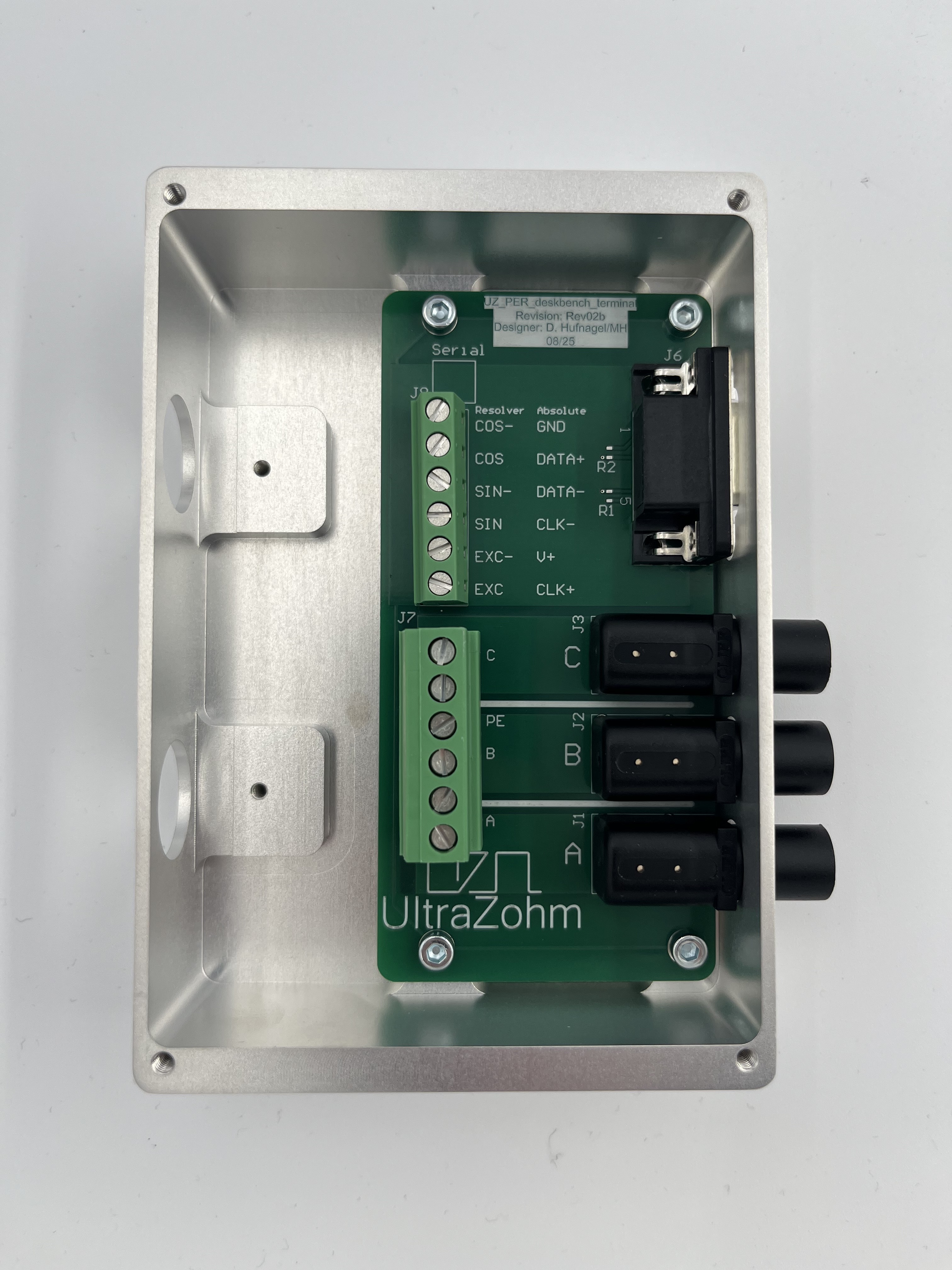
Fig. 320 uz_per_deskbench_terminal PCB Rev02 in housing#
Source#
Variants#
The PCB is available in two variants: one with an optional motor-brake connection and one without it. Currently, only the version without the brake connection is in use.
In the Rev02 variant, the clearance distances between the copper areas of phases A, B, and C have been increased to support a DC-link voltage of up to 300 V. Furthermore, two 0-Ω resistors are used to bridge specific pin pairs on the D-Sub connector, ensuring compatibility with the different pin assignments of both the Digital Resolver Rev01 and the uz_d_abs_encoder. By default, these resistors are populated.
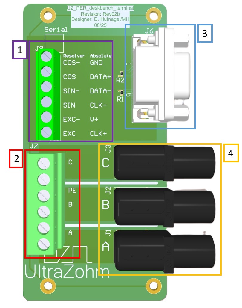
Fig. 321 Functional areas of the uz_per_deskbench_terminal PCB rev02#
Layout#
The PCB is structured by functional areas as shown in Functional areas of the uz_per_deskbench_terminal PCB rev02 above.
Terminal Connector for resolver or absolute encoder
Terminal Connector for motor
Output DSUB to UZ with Digital Resolver Rev01
Lab socket to inverter Digital Inverter Rev03
Absolute Encoder |
Resolver |
PIN DSUB 9 |
|---|---|---|
GND |
COS- |
4 |
DATA+ |
COS |
3 |
DATA- |
SIN- |
2 |
CLK- |
SIN |
1 |
V+ |
EXC- |
6 |
CLK+ |
EXC |
5 |
Color |
Pin Terminal |
PIN Inverter |
|---|---|---|
Black |
A |
Phase A |
Brown |
B |
Phase B |
Grey |
C |
Phase C |
Green-yellow |
PE |
NC |
Red |
Brake+ |
NC |
Black |
Brake- |
NC |
Downloads#
Designer#
Designed by Dennis Hufnagel(TH Nürnberg), 04/2023