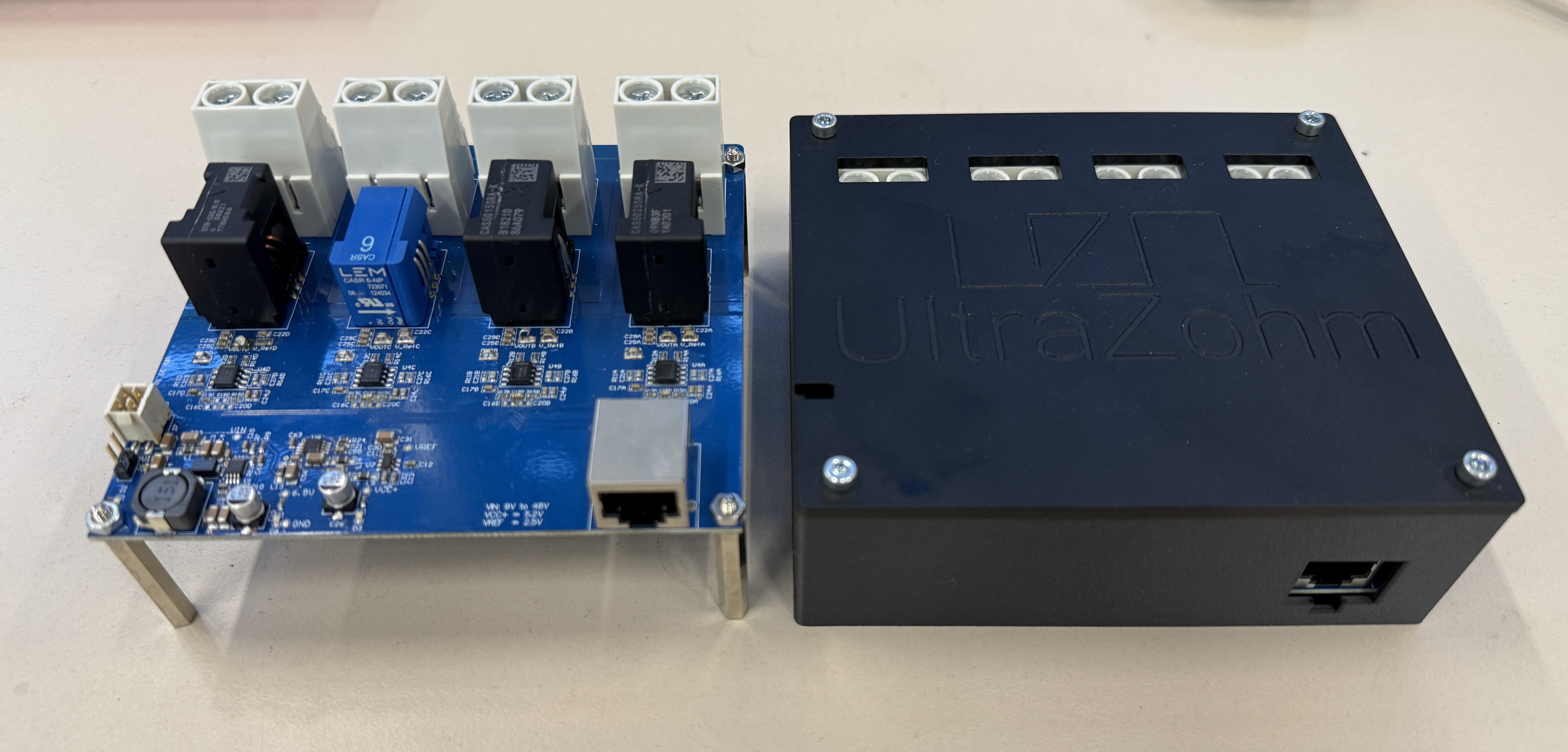
Current Measurement Box#
This section provides an overview of the analog current measurement box, including hardware details, test setup, supported configurations and findings.
Overview#
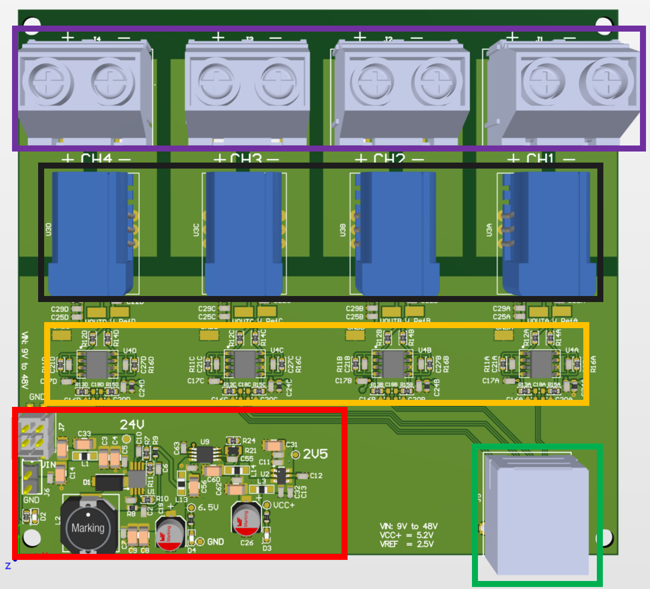
The figure above shows the top view of the current measurement PCB with highlighted functional areas:
🟪 Purple: Input screw terminals (10.16 mm pitch) for sensor current
⬛ Black: Current sensors
🟨 Orange: Fully differential operational amplifiers
🟥 Red: Power supply section with DC/DC converter (24 V to 5.12 V) and 2.5 V reference
🟩 Green: RJ45 Ethernet connector for differential output signals
Features#
4 independent current sensing channels
DC and AC measurement from 0 up to 300 kHz
Compatible with LEM CASR-NP and Sensitec CAS5000 sensors
Fully differential analog output per channel with gain of 2
Interface#
Inputs:
Supply voltage VIN: 9-48 V via 2-pin header or Samtec IPL1-102-02-L-D-K
Sensor inputs via screw terminals up to 10 mm² (≈8 AWG) (KFA-1016-10.16-2P)
Input current capability: up to 80 A peak / 57 Arms (terminal block rated)
Outputs:
4 fully differential voltage outputs via RJ45
Differential output voltage: max ±4.250 V (depending on the sensor)
Note
While the screw terminal block supports wires up to 10 mm² (≈8 AWG), operating at 80 A results in the PCB surface temperatures around 105 °C.
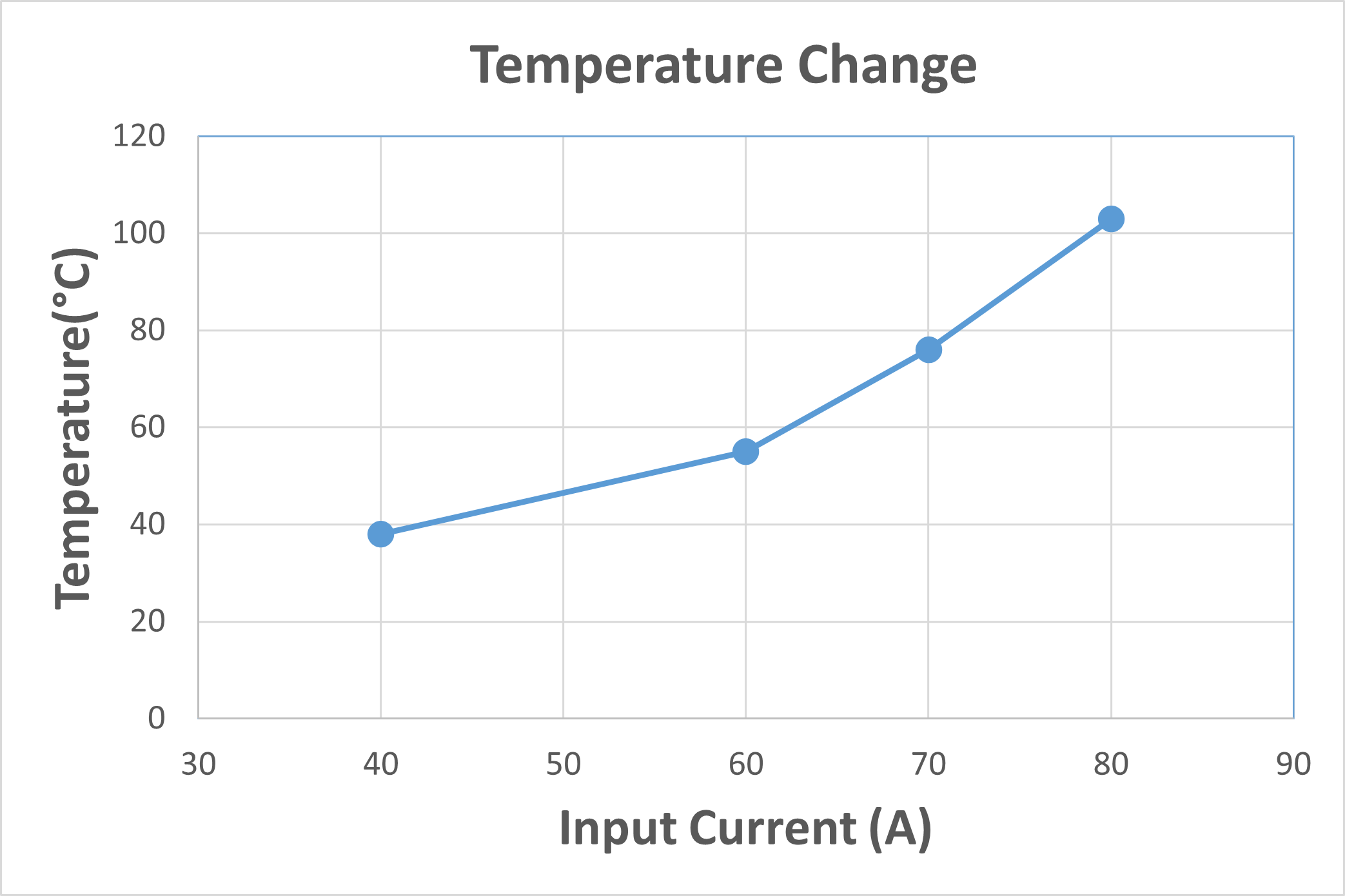
Thermal Performance#
The thermal behavior of the PCB was evaluated by applying increasing DC input current on a single phase of the primary side and measuring the surface temperature using a thermal camera. The temperature values shown in the plot below represent the hottest point observed on the PCB during each test step. The heat distribution across the primary phase trace was found to be spread relatively uniformly. As shown in the graph, at an input current of 80 A (DC), the PCB reaches a surface temperature of approximately 105 °C. Therefore 80 A should be considered as the upper limit of the current capabilities of PCB.
Clearance and Voltage Ratings#
Clearance between primary-side sensor channels (phases): 2.5 mm
Clearance between primary-side and secondary-side: 3.6 mm
Based on these clearances, the board is rated for a maximum working voltage of 500 V.
Functionality & Specifications#
Parameter |
Description |
|---|---|
VIN |
9 V to 48 V (typically 24 V) |
VCC+ Supply |
5.12 V |
Sensor Reference voltage |
2.5 V (fixed from current sensor internally) |
Number of channels |
4 |
Amplifier |
THS4521 differential op-amp, gain = 2 |
Common-mode voltage |
2.5 V (set by voltage reference IC REF35250QDBVR) |
Sensor output |
2.5 V at 0 A input current |
Differential output |
Max ±4.250 V (centered around 2.5 V) |
Input connectors |
10.16 mm pitch screw terminal blocks |
Output connectors |
RJ45 (Ethernet-style) for differential pairs |
Supported Sensors#
The analog card supports multiple current transducers with the same footprint. The last two columns indicate the unamplified sensor output voltage range for full-scale input current.
Sensor Model |
Manufacturer |
Technology |
Nominal Current (Arms) |
Range (A) |
Sensitivity (mV/A) |
Bandwidth (±3 dB) |
Sensor Output [V] (Min-Max) |
|---|---|---|---|---|---|---|---|
CASR 6-NP |
LEM |
Fluxgate |
6 |
±20 |
104.2 |
~300 kHz |
0.416 V - 4.584 V |
CASR 15-NP |
LEM |
Fluxgate |
15 |
±51 |
41.67 |
~300 kHz |
0.375 V - 4.625 V |
CASR 25-NP |
LEM |
Fluxgate |
25 |
±85 |
25.0 |
~300 kHz |
0.375 V - 4.625 V |
CASR 50-NP |
LEM |
Fluxgate |
50 |
±150 |
12.5 |
~300 kHz |
0.625 V - 4.375 V |
STB-6CAS/R/F |
Sinomags |
TMR |
6 |
±20 |
104.2 |
~400 kHz |
0.416 V - 4.584 V |
CAS5015SRA-LI |
Sensitec |
TMR |
15 |
±51 |
41.67 |
~400 kHz |
0.375 V - 4.625 V |
CAS5025SRA-LI |
Sensitec |
TMR |
25 |
±85 |
25.0 |
~400 kHz |
0.375 V - 4.625 V |
CAS5050SRA-LI |
Sensitec |
TMR |
50 |
±150 |
12.5 |
~400 kHz |
0.625 V - 4.375 V |
VCC+ Supply Adjustment#
The analog card uses the TPS7A4901 positive linear regulator to generate the VCC+ supply for the amplifier stage. The regulator output is configured using an external resistor divider according to:
Where \(V_{\text{FB}} = 1.185\,\mathrm{V}\) (datasheet)
In this design:
\(V_{\text{OUT}} = 5.12\,\mathrm{V}\) (\(R_\mathrm{2} = 10\,\mathrm{k\Omega}\), \(R_\mathrm{1} = 33.2\,\mathrm{k\Omega}\))
Why 5.12 V?#
The THS4521 op-amp has output swing limitations and cannot reach the exact power supply rails. According to its datasheet, at a 5.0 V supply, the output typically swings between ~0.1 V and ~4.7 V. So the linear output swing is around 0.1 V to 4.7 V. When using high-range sensors (CAS5015SRA-LI, CAS5025SRA-LI etc.), the amplified signal pushes the op-amp very close to these swing limits. Using a slightly elevated VCC+ (5.12 V) improves the available headroom. Therefore:
Output remains in the linear operating region
No clipping near the rails
Reliable full-scale operation with low distortion
The expected differential output from the current sensing chain is very close to the typical output swing limits of the THS4521 at a 5.0 V supply, reinforcing the need for increased supply headroom.
Note
The sensor reference voltage remains at 2.5 V regardless of the 5.12 V supply, so output offset and scaling are unaffected. Only the amplifier headroom benefits from the increased supply.
Adjust Measurement Gain#
For all types of current sensing measurements, it is recommended to configure the gain of the differential operational amplifier (THS4521) to match the expected sensor output range to the ADC input range, ideally maximizing dynamic range.
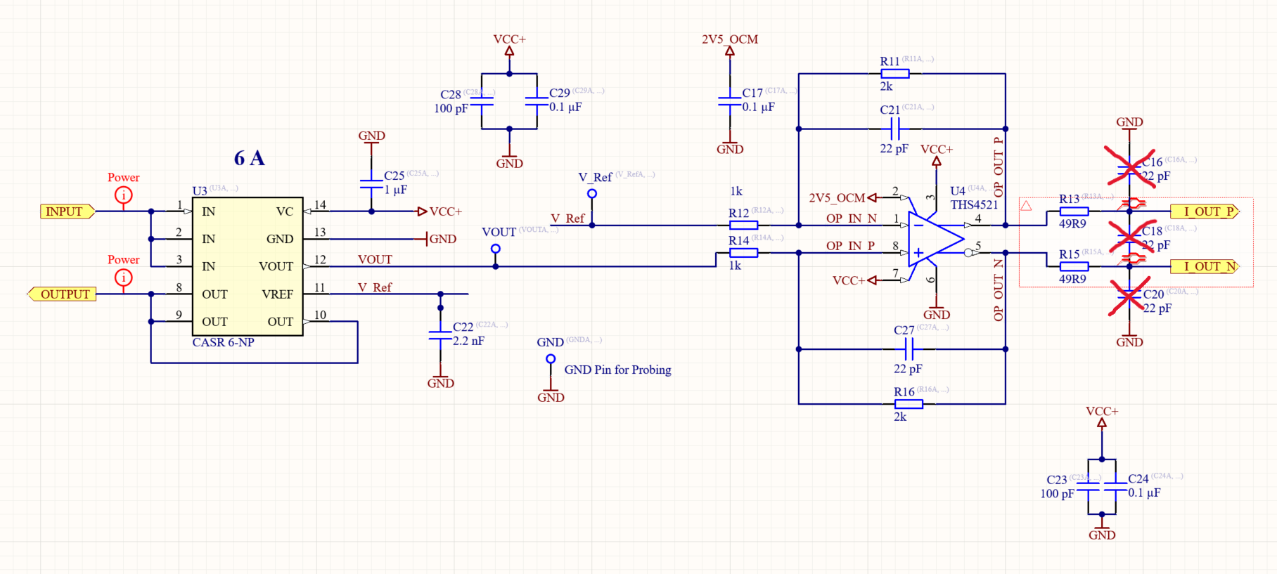
The gain is configured using external feedback resistors R11 and R12 as follows:
Ensure that R12=R14 and R11=R16 holds. This sets the overall gain of the amplifier stage to 2, amplifying the differential voltage from the sensor to match the ADC’s ±5 V input range when full-scale current is applied.
Note
Use precision resistors (0.1% or better) for R11, R12, R14, R16 to ensure consistent gain and matching across all channels.
Filters#
The analog signal path includes two types of low-pass filters: an anti-aliasing filter and an active differential low-pass filter.
1. The crossover frequency \(f_\mathrm{aliasing,-3dB}\) of the anti-aliasing filter is defined by the differential capacitor \(C_\mathrm{Diff}\) (C18 = 5.6 nF), which is populated, and the common-mode capacitors \(C_\mathrm{CM}\) (C16, C20), which are not populated during initial testing.
This anti-aliasing filter attenuates high-frequency differential-mode noise.
Additionally, \(C_\mathrm{f}\) and \(R_\mathrm{f}\) form an active first-order low-pass filter, with:
Note
As a rule of thumb, the following condition should hold:
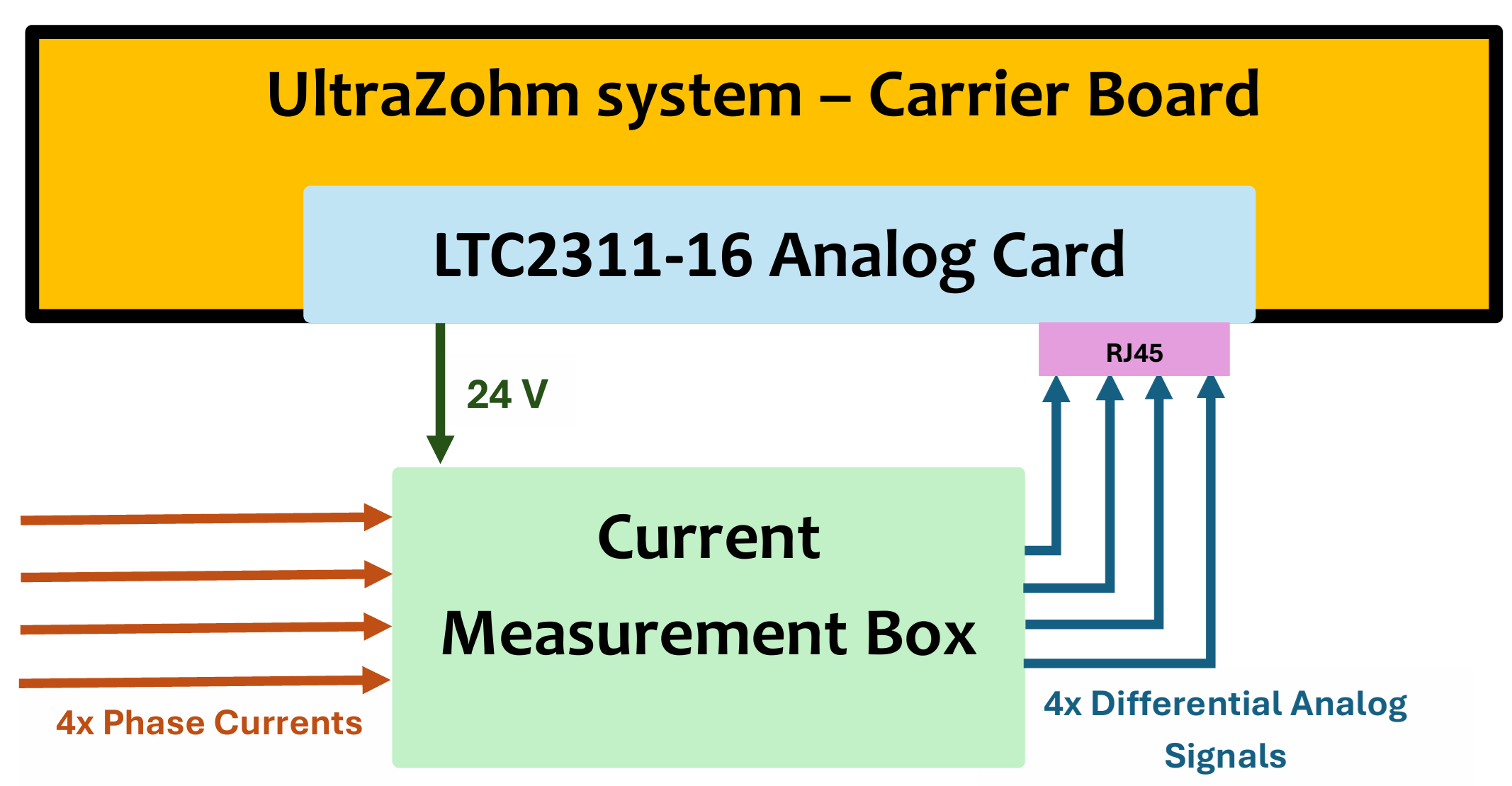
Block diagram showing the signal and power flow between the UltraZohm system carrier board, current measurement box, and the LTC2311-16 ADC card.